Reading view

There are new articles available, click to refresh the page.

No Jensen, Not All Compute is Created Equal

is in Cape Town for two weeks… email Nick at nick@chinatalk.media if you’re interested in joining a ChinaTalk meetup!

We’ve recently tried to pin down how much compute China actually has, approaching the question from both the supply and demand sides. We converged on roughly 2.5 to 2.8 million H100-equivalents. But a single aggregate figure only captures part of the picture.

Jensen on China

On Dwarkesh’s podcast last week, Jensen Huang argued that China already has enough compute to build frontier AI.

“They manufacture 60% of the world’s mainstream chips, maybe more.”

When Dwarkesh raised the gap in advanced chips, Jensen responded,

“AI is a parallel computing problem, isn’t it? Why can’t they just put 4x, 10x, as many chips together because energy’s free?”

Jensen is wrong, but that doesn’t mean people aren’t compelled by this line of reasoning. John Moolenaar, who chairs the House Select Committee on China, sent a letter to Lutnick in December proposing a rolling technical threshold that would cap Chinese aggregate AI compute at 10% of US compute capacity. It’s much more nuanced — accounting for memory and network bandwidth as part of this calculus — but ultimately seems motivated by preventing, as the letter calls it, “death by a thousand sub‐threshold chips.”

Export restrictions are a difficult line to walk, and total computing power does matter. But not all compute is created equal. The compute that can train a frontier model, serve inference on an existing one, and power your laptop are different things, and a “death by a thousand sub-threshold chips” is less concerning for the trajectory of AI than a concentration of the most important chips.

Legacy Chips Don’t Matter for AI

It’s hard to know where Jensen is getting his claim that “China manufactures 60% of the world’s mainstream chips.” Perhaps originally from a 2024 projection from previous Commerce Secretary Gina Raimondo about new legacy chip capacity coming online in China. But this is not a measure of AI compute. It includes the chips running your car’s engine management system, your washing machine’s control board, and the power electronics in an industrial motor, typically manufactured at 28nm or larger. They matter, but they are not the chips that train frontier AI. A chip in your microwave cannot do matrix multiplication for a transformer, and a 40nm microcontroller in a Chinese EV does not help run DeepSeek-V4.

The sliver of Chinese chip output that is actually AI-relevant, primarily Huawei’s Ascend line, is roughly a million chips. But even the flagship Ascend 910C (with yields of about 300-600k chips this year) delivers slightly worse than Nvidia’s H20 for training, nowhere close to a Blackwell, and much of current production still depends on a stockpile of TSMC dies acquired before controls tightened. The remainder of China’s frontier-relevant compute comes from smuggled Nvidia chips and legally imported lower-tier chips like the H20. In short, China produces lower-quality chips and still cannot manufacture as many of them as the U.S. does; for them to reach anything close to a “death by a thousand sub-threshold chips” scenario, Chinese companies would have to concentrate what compute they do have to a degree greater than any American lab — a difficult task given the vigorous competition taking place between them.

This is why FLOPs is a more honest metric than total chip count. FLOPs, or floating-point operations per second, measure how many arithmetic calculations a chip can perform in a given second, and they are the fundamental currency of AI training and inference, since every command an AI executes is ultimately a sequence of multiply-and-add operations. And the FLOPs gap between frontier and legacy chips on this metric is staggering. A single Nvidia Blackwell B200 delivers roughly 10 petaFLOPs of dense FP8 performance, while a typical 28nm automotive microcontroller delivers around 0.12 teraFLOPs of FP32, roughly twenty thousand times less.1 To put that in concrete terms, if a country had 100,000 Blackwells, its rival would need more than the absurd number of two billion legacy chips to match the same FLOPs output.
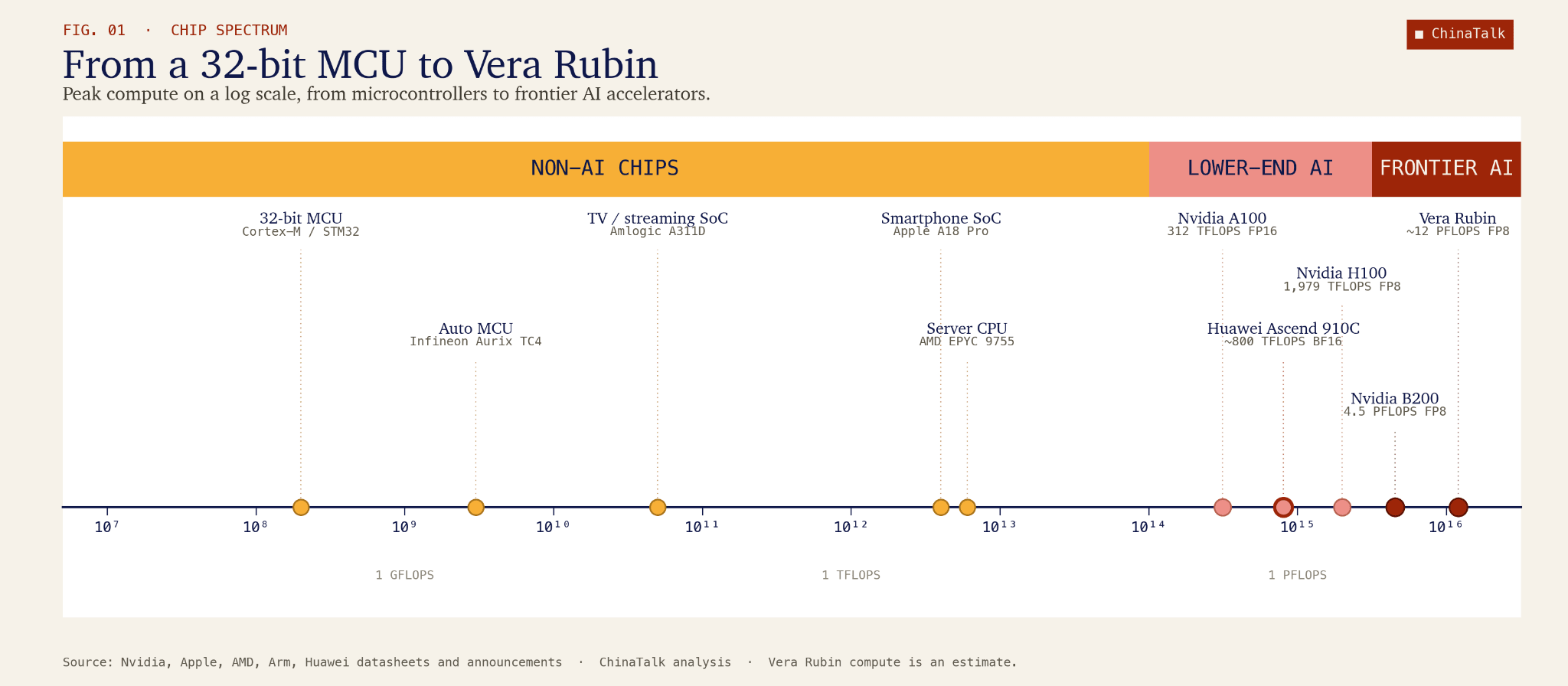
But putting mainstream legacy chips aside, if China somehow did stack up many weak AI-focused chips (like Ascends), its problems would not end at matching FLOPs.

A Tale of Two Hypothetical Countries

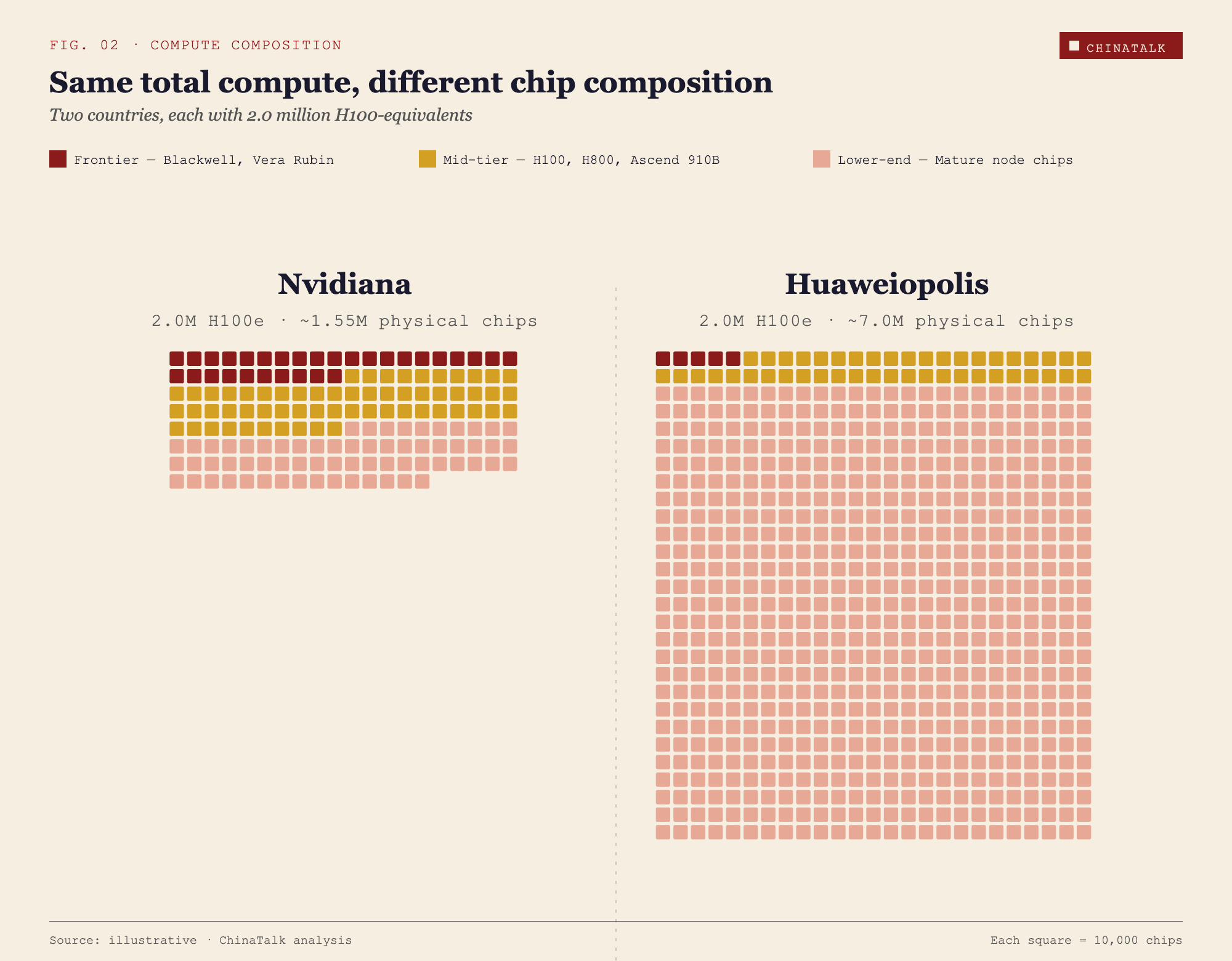
Nvidiana and Huaweiopolis each have 2 million H100-equivalents. On paper, they are peers.

Nvidiana’s stock is top-heavy and lean. Roughly 300,000 frontier chips, the Blackwells and soon-to-arrive Vera Rubins, sit at the core, tightly interconnected in a handful of purpose-built data centers that can host training runs of tens of thousands of chips in lockstep. Another 600,000 chips, the H100s and H800s, handle large-scale training and serious inference. The remainder is padded out by around 650,000 older accelerators and general-purpose silicon for lighter workloads. Total physical chip count, roughly 1.55 million.
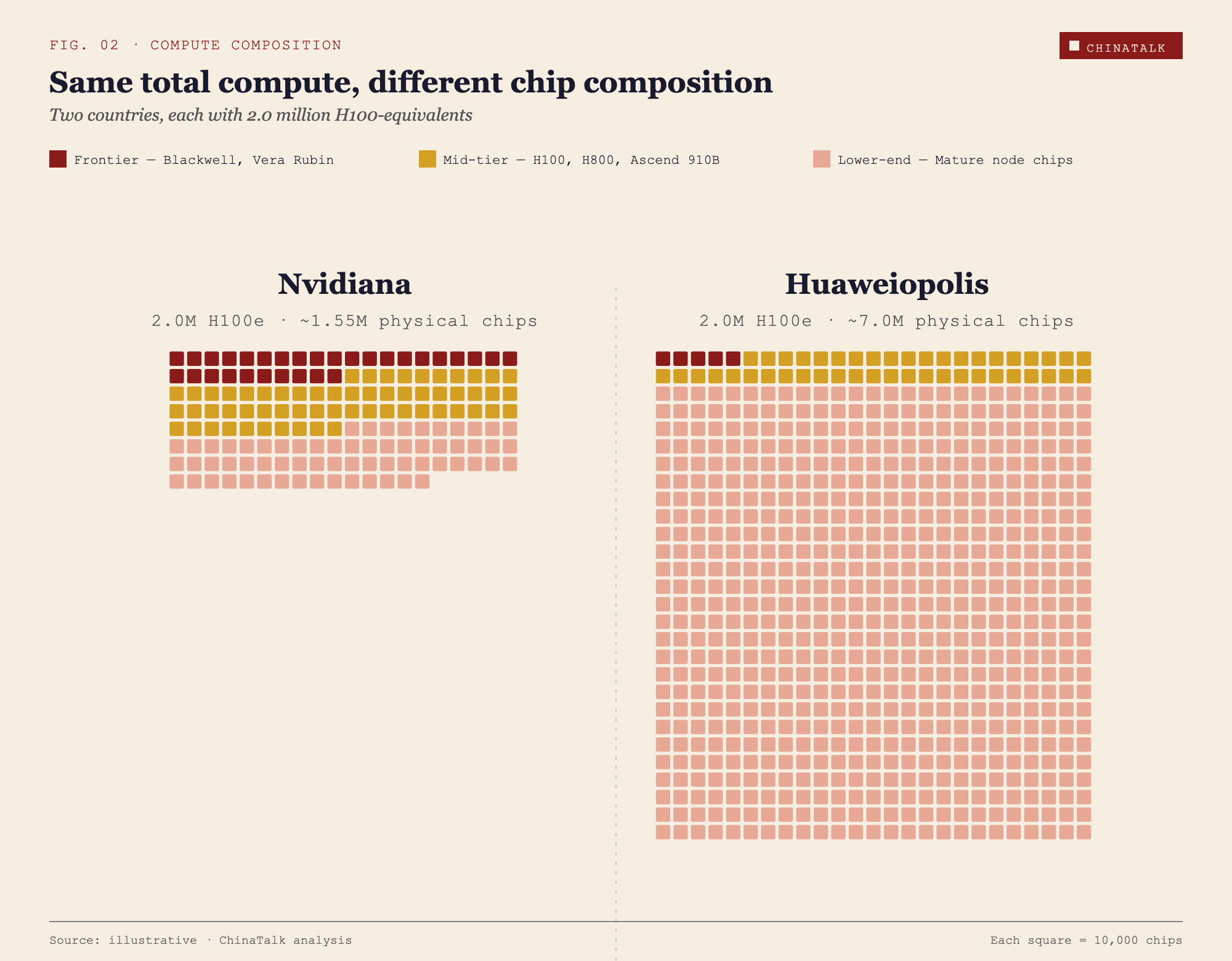
Huaweiopolis got to the same total a different way, by stacking weaker chips in enormous volume. Its top tier is thin, perhaps 50,000 frontier chips acquired before the latest round of export controls, and even those are scattered across several clusters rather than concentrated. A middle tier of around 450,000 chips, a mix of older Hopper variants and Chinese accelerators like Huawei’s Ascend 910B, is capable but constrained by weaker interconnect and memory bandwidth. The remaining mass of Huaweiopolis’s stack, close to 6.5 million chips, is older, inference-oriented chips like the H20, and repurposed general-purpose hardware. Total physical chip count, roughly 7 million — more than four times Nvidiana’s.

Nvidiana can train and serve the next generation of frontier models. Huaweiopolis cannot, and more chips will not close the gap. The difference in their AI trajectories will be substantial, even with identical FLOP counts.

Why Fewer Powerful Chips Beat Lots of Weak Chips

Huaweiopolis’s performance will lag behind for three main reasons: numerical precision, memory bandwidth, and network bandwidth.2

Numerical Precision

Older chips are not designed for the latest trends in numerical precision — that is, how finely or coarsely a chip represents numbers when doing calculations, which directly affects how much data needs to be moved and processed. Older chips, like the Hopper series, are designed to handle INT8 operations at best, meaning numbers are calculated to eight digits. Meanwhile, newer chips like the Blackwell series are designed to handle both INT8 and FP4 calculations, a jump that essentially doubles the speed of a chip. These chips can instead calculate numbers to only four digits while minimally compromising performance. By calculating half the digits, these chips have double the speed. If you are comparing chips across a standard of INT8 operations, which most studies do, then you are obfuscating the extra capability that newer chips get from being able to perform at FP4. Newer models are being trained at FP4, and inference also does not really care about less precision, meaning the capability to perform at lower numerical precision is a boon.

Memory Bandwidth

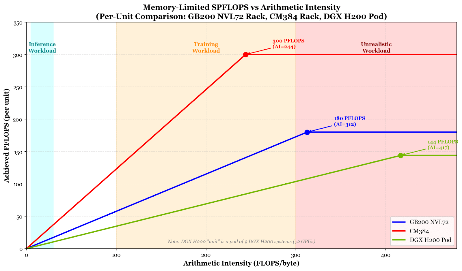
Measuring FLOPs alone also overlooks the critical importance of memory bandwidth. For most inference workloads, chip performance is not constrained by FLOPs but rather memory, since running a model means searching for and pulling billions of its stored values just to do a handful of simple calculations on each one before moving to the next. Instead of waiting for the logic to crunch numbers, the logic is waiting for the memory to fetch it numbers to crunch. A chip with ample FLOPs but insufficient memory bandwidth is like a chef with incredible knife skills but a single narrow hallway between the pantry and the kitchen, where she often has to waste time waiting in line behind the other chefs to get her ingredients. No matter how fast her hands move, the ingredients accumulate too slowly for the speed to really matter.

Frontier AI chips typically rely on high-bandwidth memory (HBM) to maximize memory bandwidth so that this downtime is minimized. Older chips use older HBM, which has worse memory bandwidth. The Hopper series uses HBM3e with a bandwidth of 4.8TB/s, whereas the Blackwell series uses newer HBM3e with a bandwidth of 8TB/s. (TB/s stands for terabytes per second, the rate at which the memory can deliver stored values to the compute units.) The newest Vera Rubin chips use HBM4 with over 22TB/s of memory bandwidth. Meanwhile, domestic Chinese chips have yet to crack HBM3; Huawei’s Ascend 910C uses (foreign-made) HBM2E with only 3.2TB/s of memory bandwidth. This means that despite Huaweiopolis’s superficial equivalence in FLOPs to Nvidiana, a large proportion of those FLOPs are unusable for inference workloads, since the logic units end up twiddling their thumbs waiting for memory, making query response times far too long.

Network Bandwidth

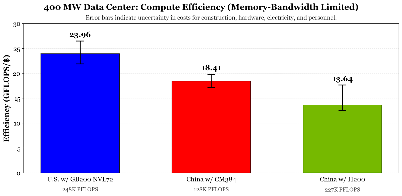
Lastly, network bandwidth — the speed at which data moves between separate chips or racks of chips — would severely limit the performance of Huaweiopolis’s cluster. Memory bandwidth is a limiting factor for within-chip communication because it determines how quickly data can move between a chip’s memory and its logic, effectively setting how fast the chip can stay fed with work. Network bandwidth — how quickly different chips can exchange data across the rack — is the limiting factor for between-chip communication, and network bandwidth is significantly slower than memory bandwidth. For an eight-chip cluster of B200s, memory bandwidth is an aggregate of 64TB/s, whereas network bandwidth is only 14.4TB/s. For training and serving inference on models, you don’t want to use network communication if you can help it because every time chips need to exchange data, they must stop and wait on one another; at scale, this turns communication into the dominant cost, meaning that adding more chips yields diminishing returns and eventually no additional performance at all.

Unfortunately for Huaweiopolis, if their strategy is to connect a massive blob of lower-quality chips to compete with a tiny cluster of higher-quality chips, they cannot succeed; network communication is unavoidable, and it will hurt. A Nvidiana cluster, with more power and memory storage per chip, can do a lot more within-chip before needing to resort to between-chip communication. A Huaweiopolis cluster will be running into this bottleneck a lot more frequently, and it will slow down operations. Particularly for training large models, where using multiple clusters of chips is necessary, the network bandwidth limitations will be crippling.

Jensen likes to dismiss this issue by arguing that “Huawei is a networking company” and dismissing the importance of HBM, but this is simply not the case. Networking will always be worse than memory bandwidth because data inside a chip moves over much shorter, more direct connections, while networking requires sending data across longer links with added coordination delays. Even God’s best NVL72 or Huawei optical fibre could not beat HBM in this battle because “beating HBM” would mean feeding the chip inputs as fast as its own memory can, which no external network can match.

FLOPs matter, but they are not the only metric. They are perhaps our best metric of comparison for now, but a proper comparison requires consideration of multiple factors. A naive equivalence on FLOPs of a Huaweiopolis cluster with a Nvidiana cluster hides the fact that the Huaweiopolis cluster will suffer in performance for both training and inference. This is not just a question of efficiency or speed. In extreme cases, the system can simply fail to train properly. Modern training requires tightly synchronized gradient updates across many chips, so if communication is too slow or inconsistent, those updates arrive late or out of step. The result is that the model is no longer being updated in a coherent direction — gradients do not reliably descend — and training can become unstable or fail to converge altogether, not just take longer or require more energy.

Conclusion

Aggregate compute matters, especially for the broad diffusion of AI across an economy. But when the question is whether a country will have the most powerful AI model, the quality and concentration of its best chips matter far more than its total headcount, and even more than total FLOPs.

There are signs that policymakers are beginning to internalize this logic. Moolenaar’s SCALE Act, introduced this week, still uses the rolling technical threshold framework but has shifted away from his earlier proposal to cap China’s aggregate compute at 10% of US capacity, which was the more aggregate-focused approach. Instead, it would permit exports only up to 110% of the performance of the best chips China can already manufacture domestically at scale, pegging the threshold to Chinese domestic capability rather than total compute. It is a narrower, more observable target, and it takes the quality-over-quantity insight more seriously than the aggregate headcount approach did.

No chip policy is going to be perfect, but the underlying logic is to focus the policy on the specific chips that matter most. We should be building enforcement around these crown jewels rather than solely around an aggregate FLOP count, and definitely not based on dubious chip counts!

To receive new posts and support our work, subscribe!

Mood Music (Jordan)

1

The B200 and MCU numbers are measured at different numerical precisions, FP8 and FP32 respectively. Lower-precision formats allow more operations per second on the same silicon, with throughput roughly doubling for each halving of precision on modern tensor cores, per Nvidia’s blog. Going from FP8 to FP32 means doubling the bit width twice, which cuts throughput by roughly a factor of four. That brings the Blackwell’s 10 petaFLOPs FP8 down to an estimated 2.5 petaFLOPs FP32, which divided by the MCU’s 0.12 teraFLOPs yields a ratio of roughly 20,000 to 1.

2

Huaweiopolis’s setup will also be significantly more expensive, but we will omit this for a purely performance-based analysis.
Fixing the GaN Problem

In the semiconductor industry, the Trump administration is striving to bring back critical technologies that slipped out of our hands decades ago. The U.S. has attracted billions of dollars in investment to stimulate cutting-edge logic manufacturing, the development of EUV lithography, and HBM production. However, the semiconductor ecosystem is a lot more than just AI chips. And if the administration wants secure supply chains, it should focus on another rising material: gallium.

Just as Pluto is technically not a planet, gallium is technically not a rare-earth element despite often being discussed in the same context. Like many rare earths, gallium is not directly mined from the Earth’s crust but rather a byproduct of aluminum extraction. Although not classified as a rare earth, the mineral plays a major role in compound semiconductors and has critical importance for the future of AI, defense, robotics, and more.

China has realized the element’s importance and has quietly shored up its supply chain while the U.S. has been asleep at the wheel. Now, the U.S. must secure this critical mineral and its downstream technologies before another lead slips from our hands.

The Problem

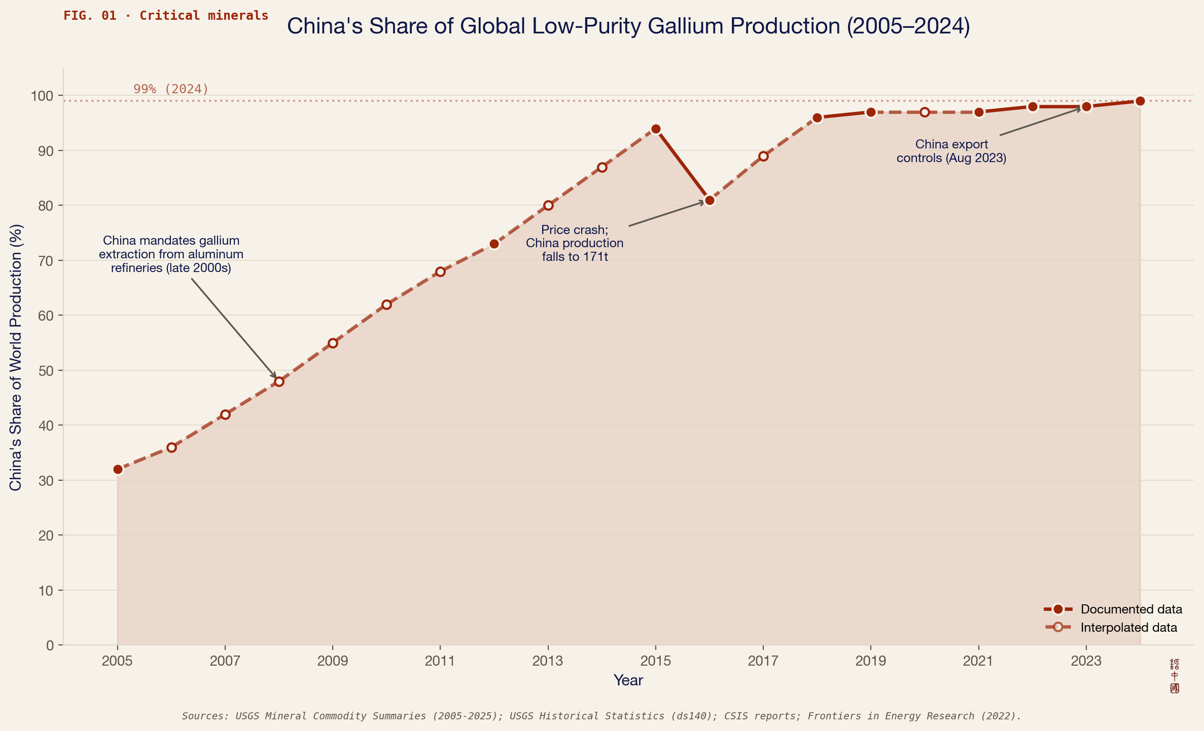
China’s recognition of gallium as a priority — both for domestic development and weaponization against adversaries — is unmistakable. As a result of their efforts, China is responsible for 99% of raw gallium production today.

Created with Claude Code.

Since the early 2000s, China has required domestic aluminum producers to also extract gallium, which has enabled the country to not just become self-sufficient but dominate the global market for gallium extraction. In the meantime, the U.S. has not shored up its supply chain insecurities, particularly in upstream extraction, leaving America vulnerable to weaponization of the mineral.

Such vulnerability is not just hypothetical. China noticed its leverage and imposed export restrictions on gallium (and the tools to extract it) since 2023. These export controls wreaked havoc on gallium prices in the global market, and firms have reported trouble in securing licenses for required gallium. As China builds up dominance over the products downstream from gallium, the United States should be worried about a future where industries are cut off from critical semiconductors and begin working now to ensure that such a threat is neutralized.

This is the current story for upstream gallium — the mineral itself. America’s dependence on China for upstream gallium has been covered excellently by other institutions like CSIS and the Atlantic Council. To address this dependence, the U.S. must actually follow up on its many ongoing projects to produce gallium domestically.

However, a less-discussed security issue is looming: the dangers facing downstream gallium — that is, the products made from gallium. China’s downstream gallium semiconductor industry has begun to encroach on the viability of American and allied companies. Instead of panicking when it’s too late, the U.S. must address its impending downstream gallium crisis in tandem with its already-existing upstream gallium problem.

The Downstream Competition

Gallium in Power Semiconductors

What is gallium used for, and why has China emphasized it so much? The mineral forms the backbone of semiconductors like gallium nitride (GaN) and gallium arsenide (GaAs) chips, which are irreplaceable for certain defense, power, and optoelectronics applications.

Gallium, from AsianScientist

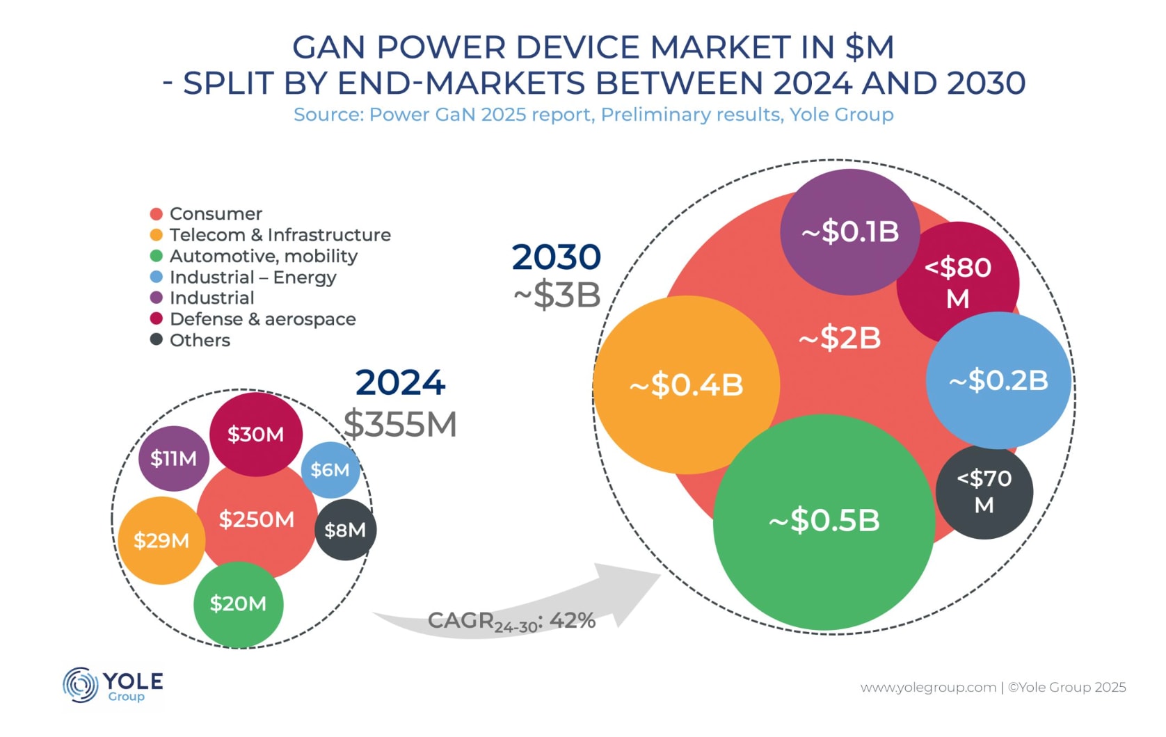
One of the most critical of these uses — and the one most under threat — is in power semiconductors, typically using gallium nitride (GaN). GaN chips used for power functions are often referred to as GaN high electron mobility transistors (HEMTs). GaN HEMTs, though currently a limited market, are increasing in popularity due to their use in EVs, motor control for robotics, and power solutions for data centers. Currently, their biggest market is the consumer end-market, focused on products like fast chargers for your laptop and phone. While consumer end-markets will likely remain GaN’s biggest cash cow, it punches above its weight in terms of irreplaceability for humanoid robotics, data centers, and EVs.

GaN, alongside silicon carbide (SiC), is considered a wide bandgap semiconductor, which endows it with properties better for power electronics compared to standard silicon. These properties include faster switching and better power efficiency. Although SiC chips are able to stand in for GaN in some contexts, GaN for power is largely irreplaceable due to its faster switching and better performance at lower voltages. Generally, SiC is used in heavy-duty applications like large industrial robotics, whereas GaN is used for lower-voltage applications like smaller humanoid robots.

BLDC motor drive inverter used in humanoid robots, which requires GaN power chips, from EPC

Innoscience’s Rise

With respect to GaN power semiconductors, the U.S. has already lost its lead and is at risk of being pushed out altogether. Like the story with solar panels and electric vehicles, the U.S. (alongside Europe) built up a lead in the “higher-value” segment of products by being a first-mover, but the lead was promptly chipped away as sprouting Chinese companies buried American firms with unbeatable prices.

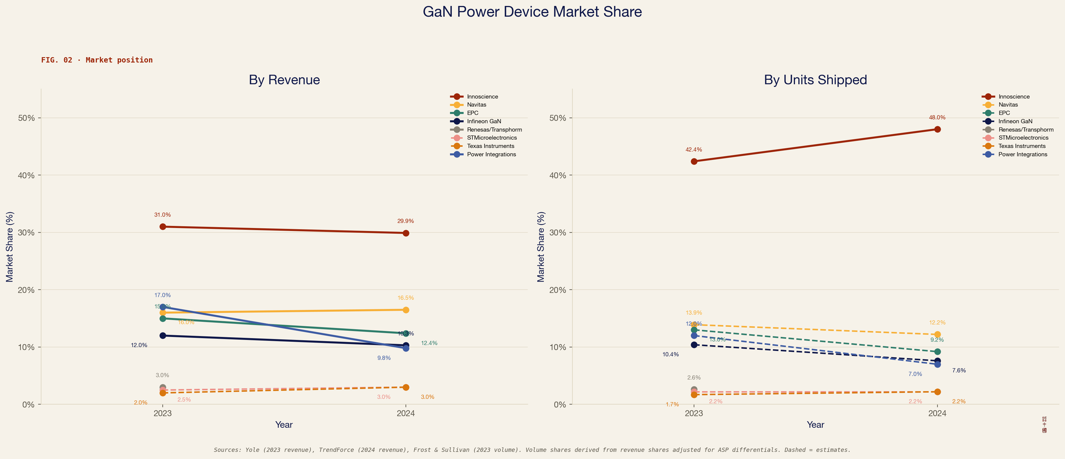
Here, the main competitor is Innoscience (英诺赛科), a Suzhou-based GaN integrated device manufacturer (IDM), whose prices are nearly 50% lower than competitors’. As a result, Innoscience now leads the global market for power GaN chips, beating out the American Navitas and EPC and German Infineon. Other players like STMicroelectronics and Onsemi have bent the knee to Innoscience by giving up packaging expertise, system integration, and their own manufacturing capacity in exchange for access to Innoscience’s production facilities in China.

As Innoscience continues to expand capacity, the situation risks shifting from one of market dominance to one of market monopolization. If trends continue, competition in the GaN power market will become a fiction, constituting a national security threat to the U.S.

Created with Claude Code.

So, how is Innoscience so much better than its competitors? The answer boils down to the synergy of in-house manufacturing, a stomach for unprofitability, government support, and genuine innovation.

In the GaN market, AMD co-founder Jerry Sanders’s adage holds true: real men have fabs. After Innoscience, the other two leading GaN makers include the American companies Navitas and EPC. Both are fabless. Both must rely on external foundries for their chips, which increases the cost of their final products.1

From the beginning, Innoscience decided to spend the money on R&D to make its own fabs, and its bet has paid off. Both Navitas and EPC have relied on TSMC for its fabrication, but TSMC is now exiting the GaN market entirely. Now, their business is getting punted off to Taiwan’s Powerchip (PSMC) and American GlobalFoundries because TSMC realized its capacity was better used for the more lucrative AI chip market.

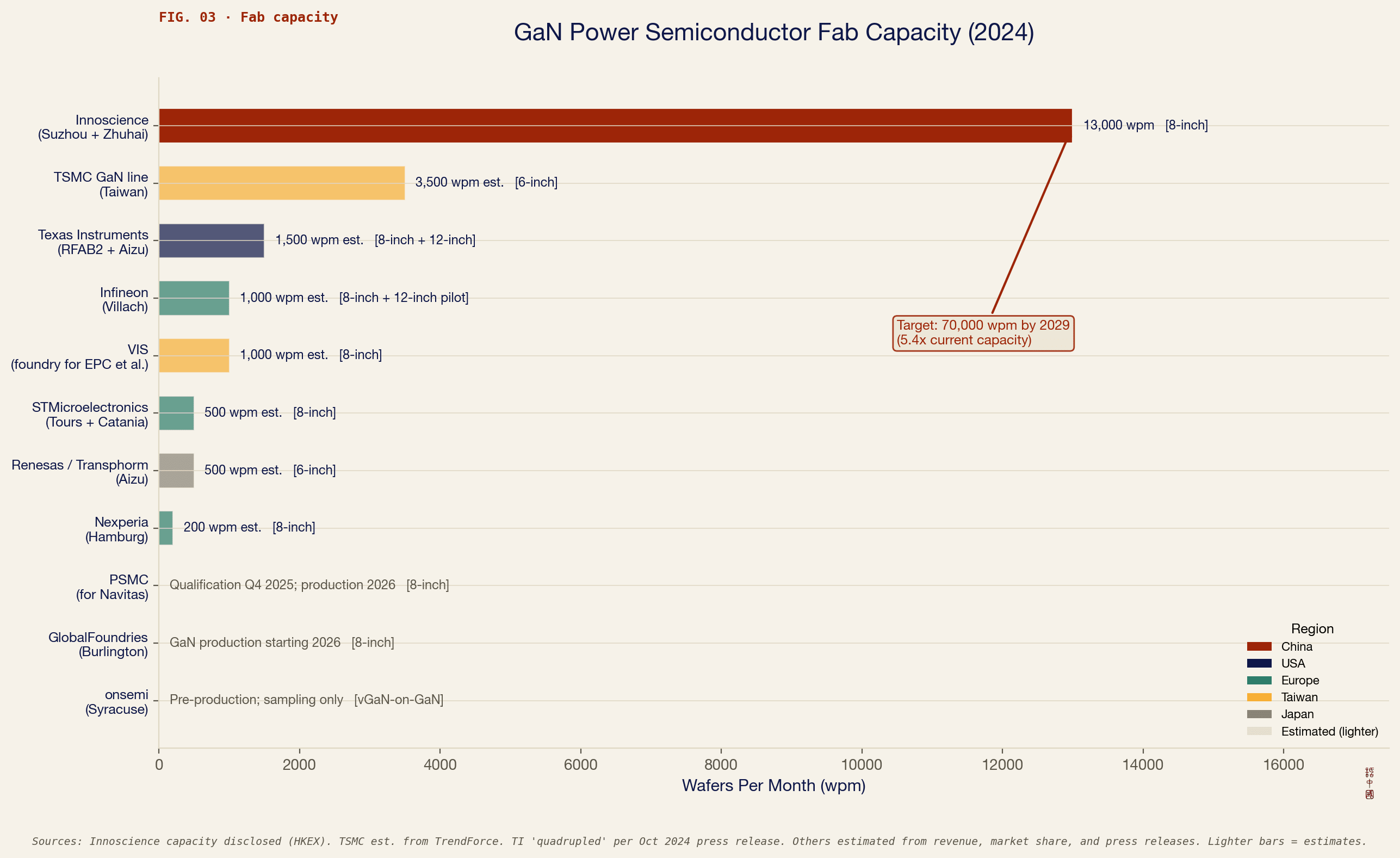
Fab capacity for GaN is trending toward Innoscience holding all the keys. By being the first to mass-produce 200mm GaN wafers, the unit economics are in Innoscience’s favor. Compared to the previous standard of 150mm wafers, 200mm wafers allow for up to 80% more chip output at 60 to 70% of the cost. Further, by being first to the scene, Innoscience has had more time to perfect its process, achieving a yield of about 97% whereas others are stuck below 90%. Innoscience’s capacity also blows competitors out of the water, producing nearly four times as many wafers as second-place TSMC. With Innoscience having no intentions to slow down, the unit economics will just get better and better for the Chinese IDM and worse and worse for everyone else.

Created with Claude Code.

Companies like Onsemi and STMicroelectronics realize that the cheapest way to fabricate their designs is through Innoscience, creating a dynamic that essentially positions Innoscience as the TSMC of GaN. The question now is how much longer can Navitas and EPC find fabs that aren’t Innoscience to fabricate for them? And then in the long term, why would Innoscience ever want to fabricate for a direct competitor when it could instead monopolize the GaN power market? Even for Onsemi and STMicroelectronics, after market consolidation, Innoscience may devour its children.

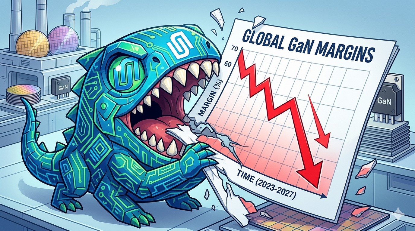
Innoscience was able to become the greatest GaN company by being willing to stomach unprofitability. In 2021, the company was operating with a gross margin of over negative 266%. Unlike Western companies, Innoscience — and its funders — have been willing to eat bitterness while it figured out its manufacturing process, increasing yield and expanding capacity. American markets do not have the same willingness. Other GaN makers have been incentivized to maximize profit margins in the short run while Innoscience chased viability over the long run, leading to where we are now.

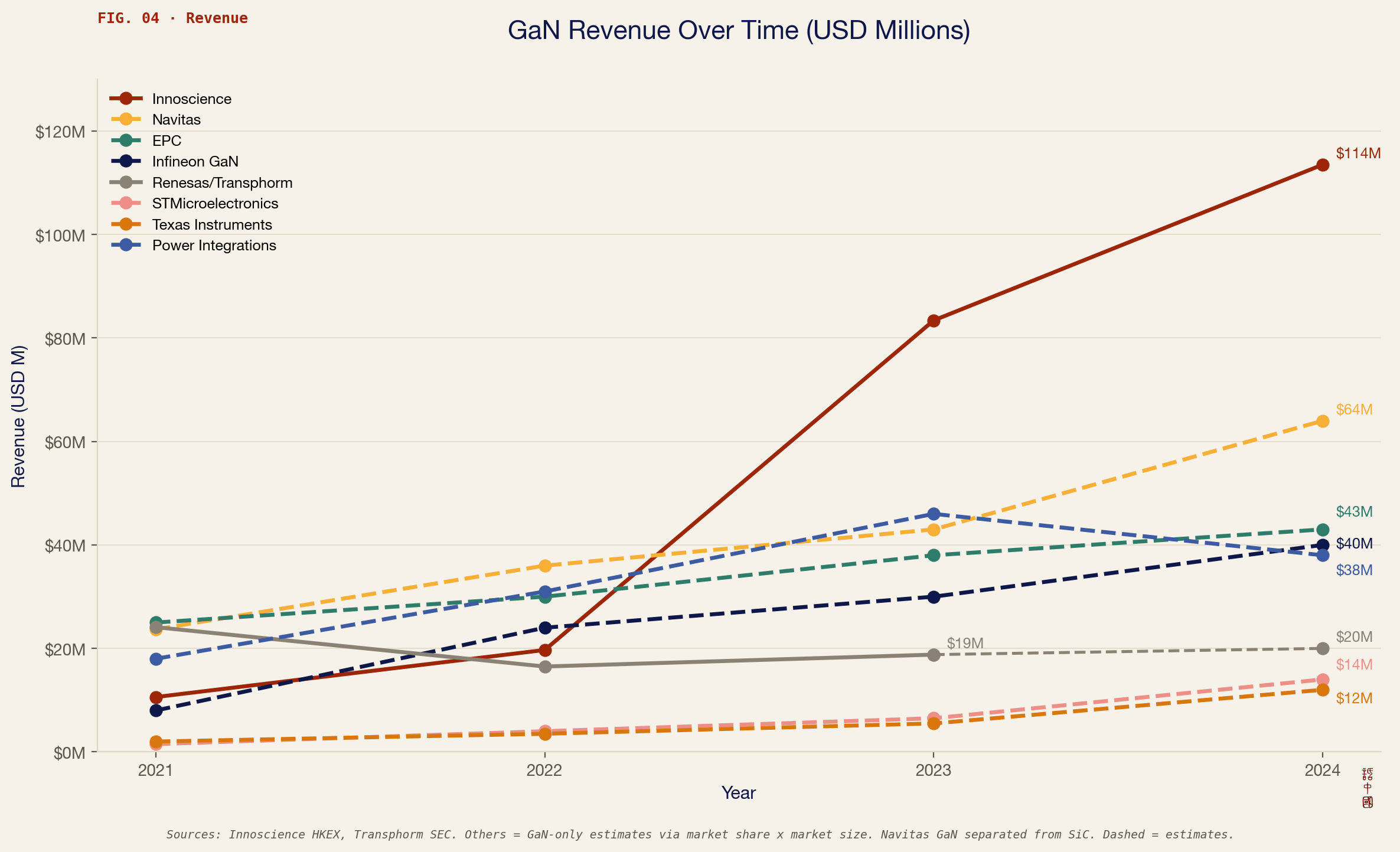
Now, Innoscience has been able to capitalize on its high-yield manufacturing process and exploding demand for GaN for high-tech applications to achieve positive margins for the first time in its history. Although the company likely won’t turn a profit until 2027, the upward revenue trend contrasts Innoscience with that of other GaN players. (Quarterly revenue from GaN sales alone is not available for some companies.) And if Innoscience was not deterred by negative margins in its early years, the company will most definitely not be deterred now.

Created with Claude Code.

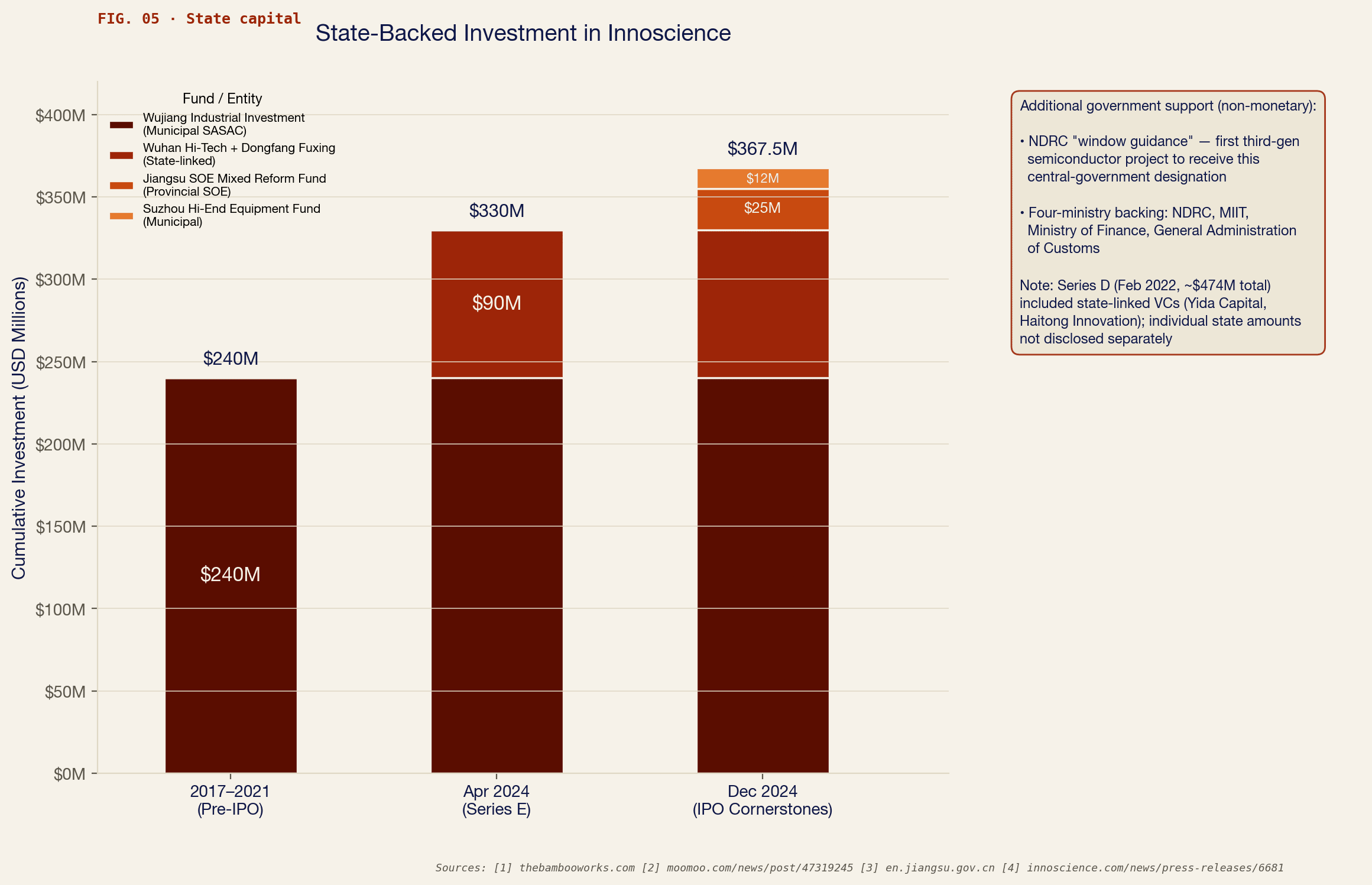
Part of Innoscience’s perseverance in the face of negative margins is due to assistance from government subsidies. The combination of investments from national and provincial state-backed funds has totalled over 350 million dollars of financial support at minimum for the then-burgeoning Innoscience. That is more than double the company’s gross losses since 2021. By the time of its IPO in 2024, the company had established enough capacity and was already poised as the best option for large-scale GaN manufacturing. Other companies like STMicroelectronics realized this, and they decided to become a cornerstone investor in Innoscience with a $50 million investment and further fund the GaN giant.

Created with Claude Code.

But before we lazily blame the evaporation of Western market share on government subsidies, we must reckon with the reality that Innoscience has also simply played better than the U.S. Competition in the GaN power market is more intense for individual voltage ranges. Some companies, like EPC, focus only on the sub-350V range. (Products in the sub-100V range are used for motors in humanoid robots, sensors and ADAS for electric vehicles, and motherboard power conversions in data centers.) Most companies expand that focus up to 650V or 700V. However, Innoscience is the only company that both designs and manufactures GaN power chips across the whole spectrum, from 15V up to 1200V.

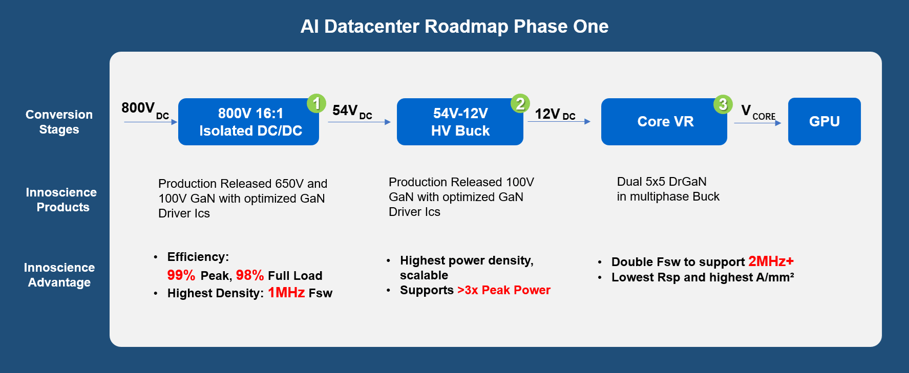
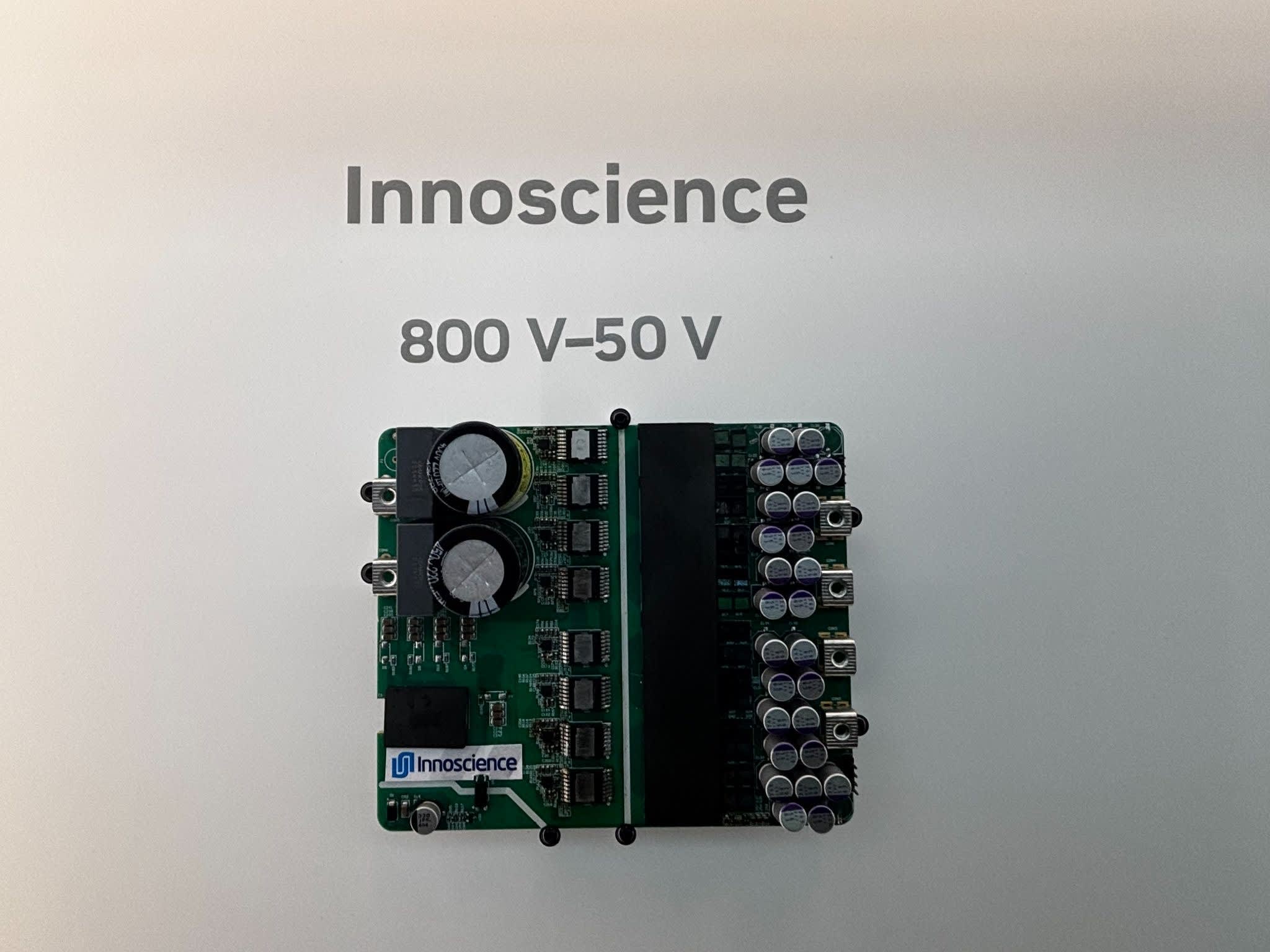
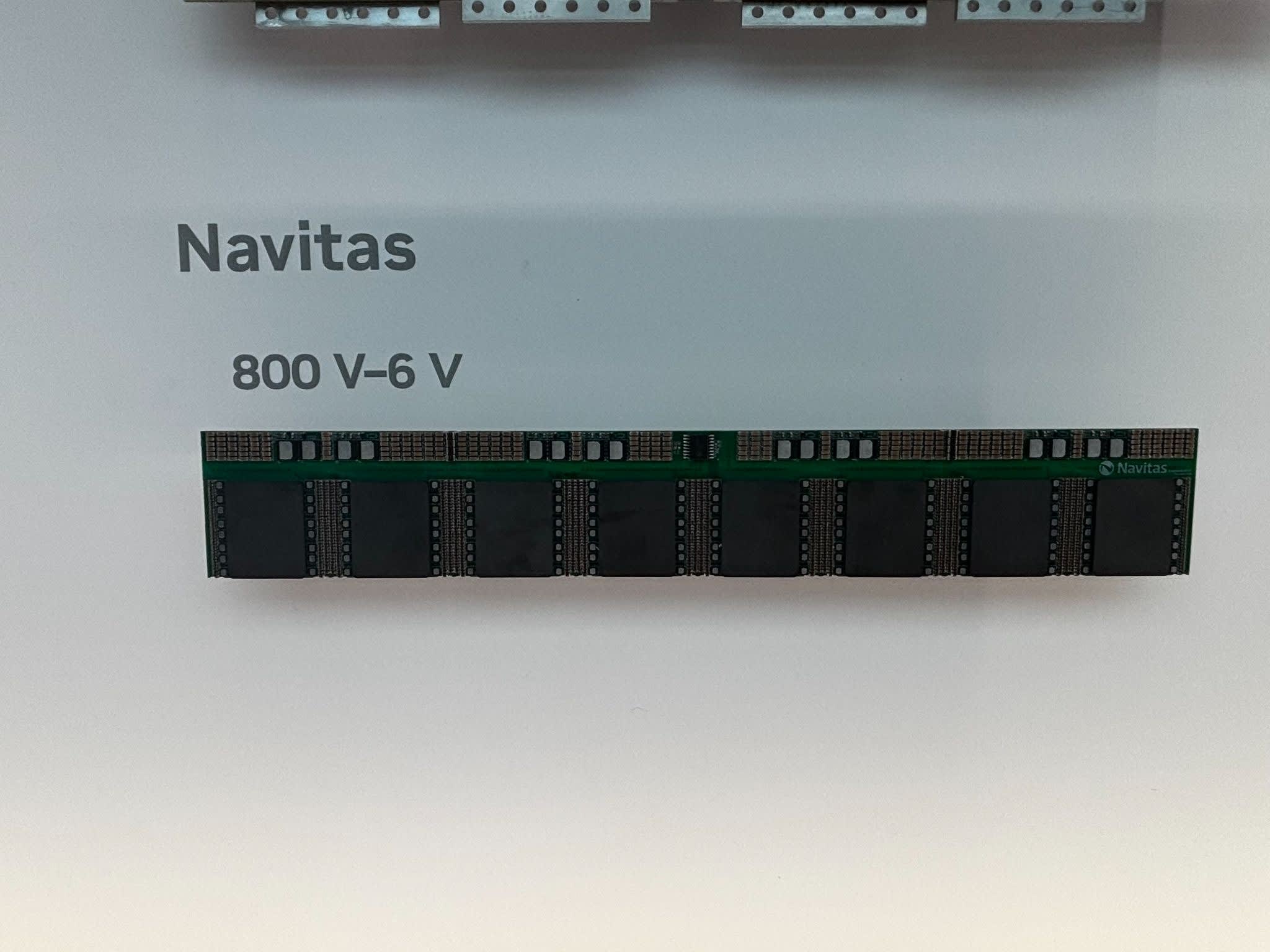
And they are not low-quality chips, either. For example, Innoscience designs and produces 650V and 100V GaN products for rack-level power conversion in AI data centers. Innovation in this increasingly critical segment enabled Innoscience to become Nvidia’s sole Chinese partner for this power architecture. The 800 VDC power architecture is touted as the best option for the “next generation of AI factories” because it allows better power efficiency and less reliance on copper cables. Although large companies like Nvidia will always qualify more than one supplier for diversification, Innoscience will likely emerge as a primary supplier if its prices and quality remain preeminent.

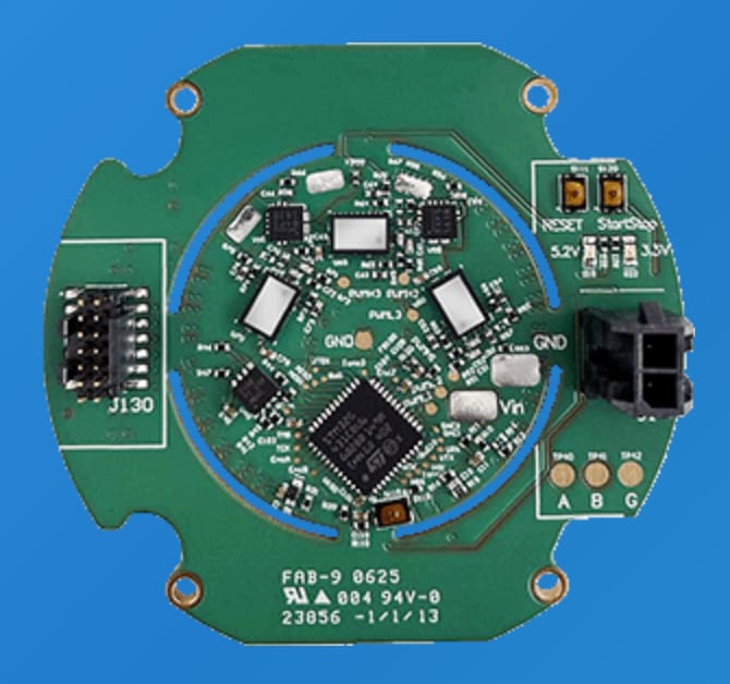
Innoscience’s 800 VDC data center reference design. Photo taken at GTC.

Lest I risk fearmongering, it is important to note that none of these 800 VDC GaN designs by any company have been qualified as of this piece’s publication. They are all simply reference designs that Nvidia has requested from these companies. A rudimentary analysis also suggests that Innoscience’s competitors have created better products for this application; for example, Navitas’s product supports an output of down to 6 V, suggesting better capabilities for handling high current. It is unclear how important this functionality is and what the cost differential is for these products. If any reader with a background in GaN would like to provide answers, please comment or reach out to aqib@chinatalk.media.

Navitas’s Product. Photo taken at GTC.

Regardless, such innovation cannot be swept aside and blamed on government subsidies; the U.S. must contend with Innoscience as a company with the ability to both produce at scale and innovate. These characteristics enabled Innoscience to establish its partnership with Nvidia (and now Google) for the future of AI data centers.

And regardless of the extent of government subsidies enabling Innoscience’s rise, the U.S. cannot just call foul play and say it isn’t fair. There is no referee. We must take fate into our own hands and fix the problem ourselves. The U.S. has prided itself on government programs such as DARPA shepherding critical technologies like GPS and the Internet before they were profitable. Can we not do the same for manufacturing critical technologies like GaN?

We now find ourselves in a position where the snowball is forming. If we do not prevent it from getting bigger, makers of robots, EVs, and data centers may reasonably be dependent on a single Chinese company for its power chips. Do we seriously believe these technologies will become less important in the future? In the next trade war or diplomatic spat, this is worrying leverage that China could use to bottleneck critical industries. Does this not mean we should be trying to stimulate GaN production, not throw its carcass to the vultures?

The Solution

Fortunately, it is easier to fix the problem now, when we still have some GaN players, compared to later, when the outcome is set in stone. To ensure the U.S. is not overreliant on China for critical GaN products, we must support allied industry to make producing GaN a profitable venture. We should perhaps limit competition in the short term to create healthy competition and stable supply chains in the long term. This does not mean the extermination of Innoscience, but rather the protection of market competition.

Policy should also recognize its limitations, however. The U.S. cannot and should not spend obscene amounts of money to compete with China on capacity. Instead, we must focus on winning on efficiency, innovation, and other methods that give us the edge besides raw buildouts.

Patent Infringement Cases

The quickest relief is through the judiciary. Both EPC and Infineon have filed patent infringement cases against Innoscience, and the results of those cases could limit Innoscience’s ability to compete in the American market. Although EPC’s claims were invalidated by the USPTO, import restrictions imposed by the ITC continue to be enforced. The Infineon case will be finally decided on May 7 by the ITC as well.

The ITC’s determinations, however, will not be a panacea. The patent infringement punishments only apply to certain products, and Innoscience would be able to design around them to continue to sell in the U.S. Further, the determinations would not be able to restrict finished products containing Innoscience chips. Especially when the current money makers — consumer end-products — are largely produced in China, the case determinations may not produce a serious impact. This route is also not a policy position, as the judiciary should not bend the rule of law for policy goals.

The Race to 300mm

Outside of the judiciary, the U.S. can support innovation and the commercialization of the next generation of GaN power semiconductors. Here, the best options for champions are Texas Instruments and Infineon. Both companies have dedicated foundry space for GaN power semiconductors, and both have piloted the production of 300mm GaN wafers. Where Innoscience was able to achieve superiority in unit economics from the shift from 150mm to 200mm wafers, TI and Infineon can perhaps achieve it in the shift from 200mm to 300mm.

However, the gains from 200mm to 300mm may not be as large as the gains from 150mm to 200mm. Although 300mm wafers produce about 2.25 times as many chips per wafer compared to 200mm, the throughput for processing may not be as high. For epitaxy, 300mm wafers currently require single-batch processing due to strict requirements for wafer uniformity and robustness, whereas 200mm wafers allow for multi-batch processing. Development of multi-batch 300mm wafer tools is almost certainly ongoing, but no progress is yet visible. The overall cost savings and throughput advantages of the 300mm transition are still unknown, but they may not be as impressive as the previous 200mm transition. The step to 300mm is a step toward the ultimate objective for GaN manufacturing — cost-parity with silicon — and it is an important step toward reducing dependence on Innoscience. However, it is not a panacea.

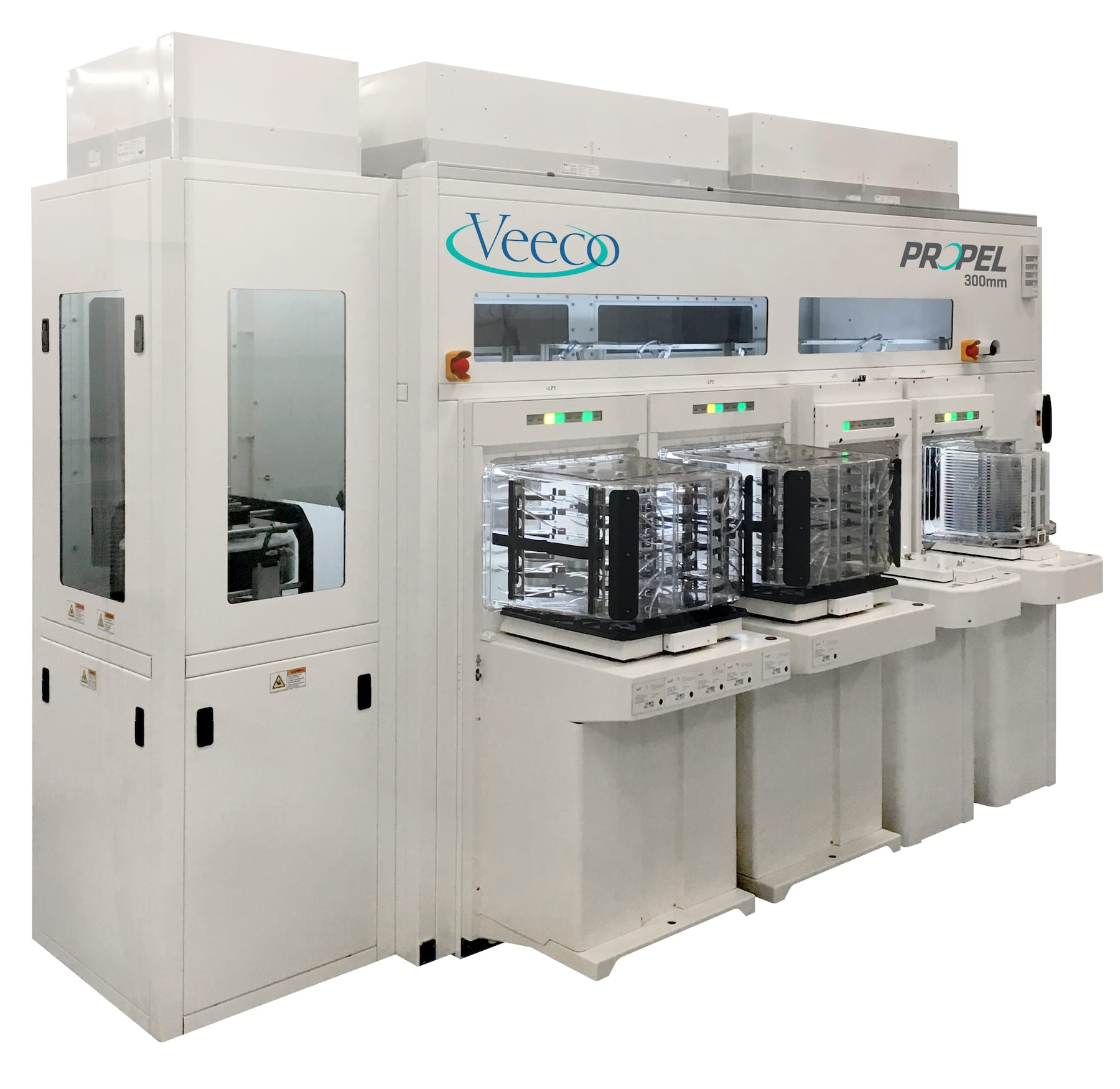
America’s export controls on the metal-organic chemical vapor deposition (MOCVD) tools required for GaN epitaxy (ECCN 3B001 a.2.) may enable the 300mm wafer lead to be enduring. Infineon and TI have been able to achieve pilot production because they have been able to purchase the relevant MOCVD equipment from the German AIXTRON and American Veeco, whereas Innoscience must wait for domestic suppliers like AMEC to develop a solution. AMEC has no visible progress toward 300mm GaN, so export controls will perhaps give TI and Infineon more time to develop and mature process flows for 300mm GaN.

Veeco’s Propel 300mm GaN MOCVD System, from Veeco

To goad TI and Infineon on, the U.S. may fund projects through the CHIPS Act to support the quicker construction (or conversion) and operation of 300mm GaN fabs. By accelerating the timeline to mass production, homegrown companies will more quickly improve yields and unit economics so Innoscience’s explosive capacity expansion would not be so oppressive. We cannot build as much as Innoscience, but perhaps we can build better.

Ecosystem Stickiness

The most enduring solution would be to create ecosystem “stickiness” for end-customers so that they are more locked into purchasing from allied companies. The West again has an inherent advantage here, with allied GaN makers (mainly U.S.-based Texas Instruments and Germany’s Infineon) being IDMs across the semiconductor stack; unlike Innoscience, they do not solely focus on GaN.

For end uses more complicated than fast chargers (e.g., data centers and robotics), GaN becomes less of a commodity and more a question of integrated solutions and technical capabilities. End customers would be more willing to work with GaN suppliers that could tailor their manufacturing solutions to the customers’ power architecture, which presents an opportunity to reduce the importance of Innoscience’s price lead.

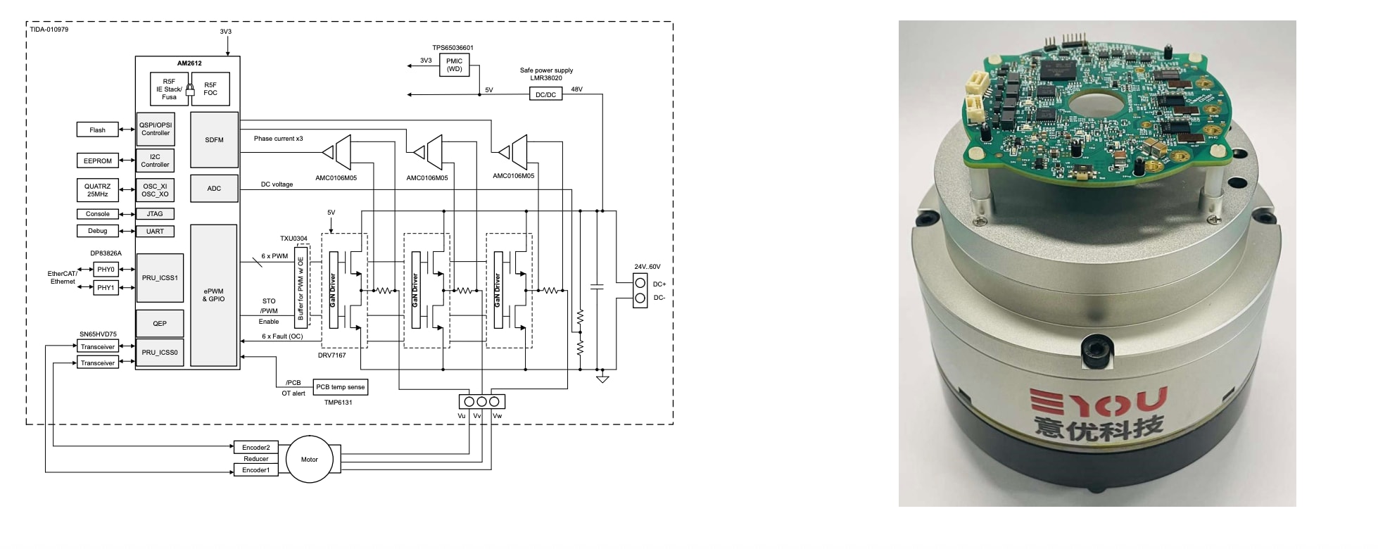
For example, when a company wants to purchase a GaN power HEMT for their humanoid robot, they should be incentivized to purchase a system, not just the product. If they are already using a TI MCU, it should pair best with TI’s gate driver ICs, TI’s sensor chips, and TI’s GaN HEMTs. By contrast, there is no such thing as an Innoscience MCU. When the full-stack comes with so many advantages, customers are incentivized and better served by sticking with TI, rather than considering redesigns to drop in a cheaper Innoscience product.

Innoscience simply does not have this ecosystem capital outside the GaN stack, and unless they quickly partner with Chinese companies across the stack, they will not accumulate such capital soon. Currently, they must rely on products from companies like TI and Taiwan’s YAGEO for reference designs of motor drives.

To capitalize on this ecosystem advantage, the U.S. could consider providing modest funding for better open reference designs for applications like robotic motors, EV onboard chargers, and data center power topologies. Companies are already incentivized to pursue this, and TI already does this well, but coordinated government funding could reduce barriers and promote better designs. If the U.S. produces powerful reference designs that perform well with potential robotics MCUs, data center power topologies, POL parameters, and vehicle architectures, then end-customers may not care about the marginal savings of Innoscience’s GaN HEMTs.

Reference Design and Picture of TIDA-010979, a driver for humanoid robot joints that uses TI MCUs, GaN drivers, etc., from Texas Instruments

The primary source of pessimism with this strategy, however, is that American reference designs may not matter if the end-customers are Chinese. If Unitree and BYD are the main end-customers, they will likely work with Chinese MCUs (like ARTERY) and be incentivized to work within the Chinese ecosystem. The American GaN market will miss out. This is not a fait accompli, however. Chinese carmakers like Changan Automobile have opted for American Navitas GaN chips for their onboard chargers, meaning Chinese OEMs can be incentivized to pick American products over Chinese ones.

Further, larger companies like hyperscalers tend to have their own engineers who do not need to rely on the easy reference designs given to them; they make bespoke designs in house and take the best products for each segment, prioritizing cost savings and performance over ease of use.

Still, funding design is significantly cheaper than funding factories, and better reference designs may trickle down to benefits for start-ups in the robotics industry where the major players have yet to calcify.

Flexible Fabs

Lastly, though most vaguely, the U.S. should incentivize companies to make it as easy as possible to convert legacy fabs into GaN fabs if the need arises, just as we did with factories during World War 2. Although this would mostly be easy, as GaN wafers can be processed by the same equipment used in depreciated legacy fabs, the biggest obstacle would be ramping up the epitaxy for GaN wafers. In this case, possible options include encouraging a GaN wafer stockpile or promoting expedited production of MOCVD equipment for GaN epitaxy.

Conclusion

The U.S. is largely aware of its upstream gallium dependency, and 99% dependence is a difficult ditch to climb out from. But let’s ensure that we do not fall into the same ditch when it comes to GaN.

The U.S. can accomplish long-term viability in the GaN market now before Innoscience makes it too difficult. We can accomplish this through innovation and flexibility, not expensive buildouts, via the pursuit of 300mm wafer adoption, ecosystem stickiness, and flexible fabs. These are not the only tools in the toolbox, but they are feasible options that the U.S. government could readily pursue.

We also do not need — and probably should not want — to banish Innoscience. American and allied companies like Onsemi and STMicroelectronics work with Innoscience, and punishing one would be punishing the whole lot. Instead, we should focus on preventing Innoscience from becoming a monopoly and encourage companies to work within the American ecosystem instead of compelling them to settle for a Chinese one. A world with Innoscience and at least one allied viable alternative is a win.

Instead of sleeping at the wheel (again), the U.S. can prevent GaN from going the way of solar panels and EVs. If we want to secure our supply chains, we can start with GaN.

To receive new posts and support our work, subscribe!

The author would like to thank several GaN industry executives for their contributions to this piece.

1

For those wondering why the fabless business model does not bring efficiency games, the reason is the real efficiency gains come from fabless firms relying on a pure-play foundry. In this case, the foundry can maximize unit economics and pass on savings to fabless firms. In GaN, this is not the case because of the small size of the GaN market. Fabs like TSMC are not incentivized to make GaN in large quantities or on large wafers, meaning the savings passed on are minimal. Innoscience’s model reflects the philosophy of being the size of a large pure-play foundry that will be serviceable in the future though a money-loser now.

Should the US Buy from CXMT?

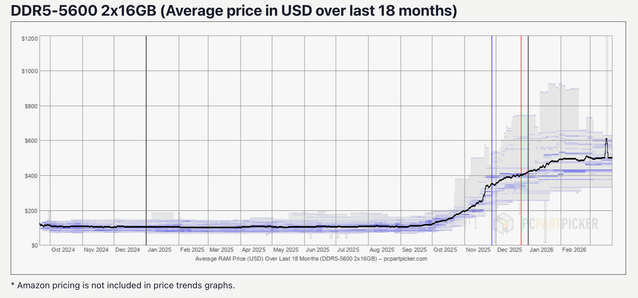
The “RAMageddon” is here. Tears roll down gamers’ cheeks as AI ruins DDR5 prices. People are even giving RAM as wedding presents. Why is memory going to the moon, and what are the geopolitical implications?

Source: PCPartPicker

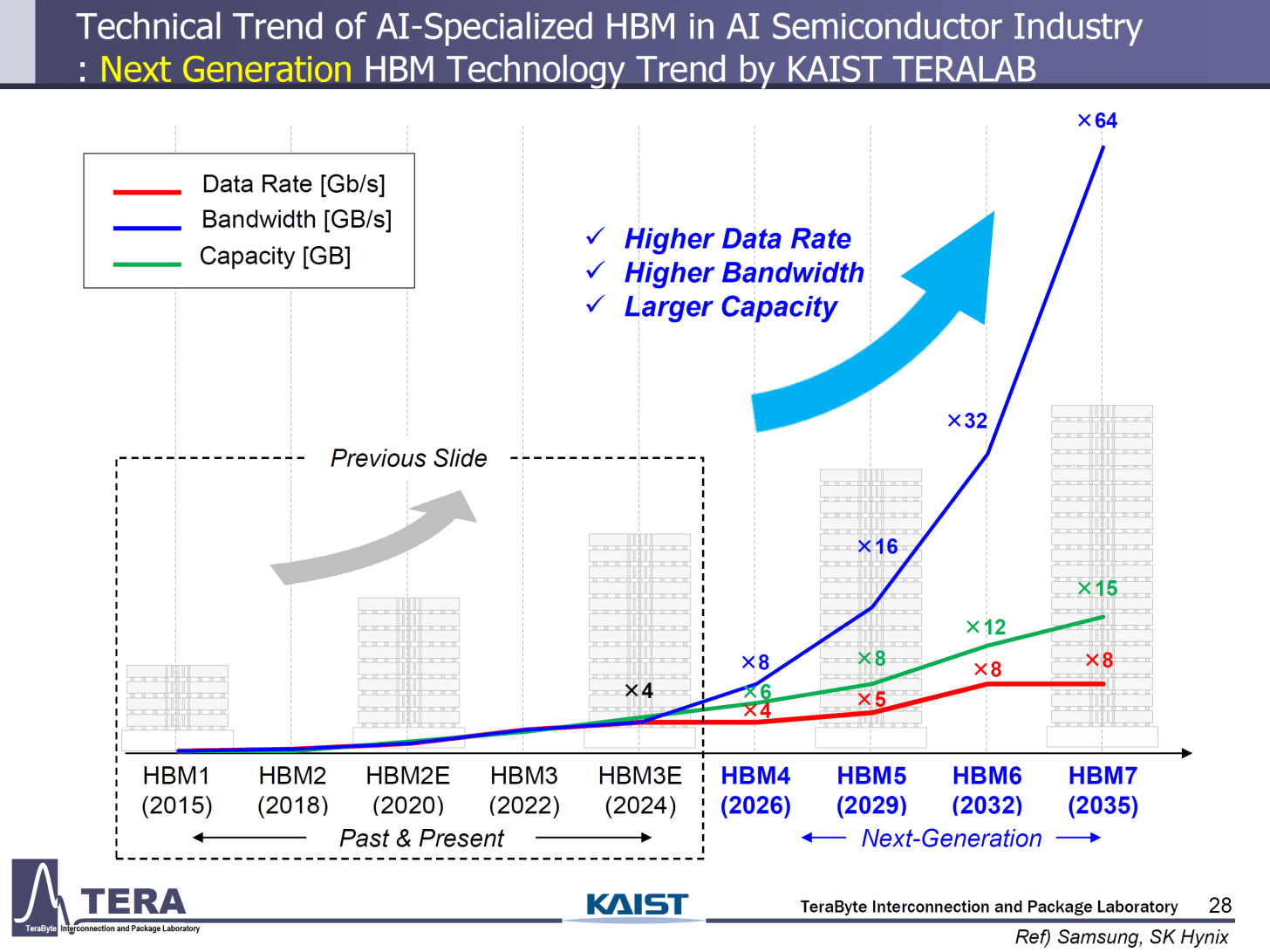
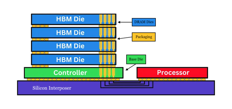
The Big Three memory makers — SK Hynix, Samsung, and Micron — have dedicated increasing capacity to memory for AI, or HBM. High-bandwidth memory (HBM) is a product that stacks multiple DRAM dies for AI memory. The increased allocation toward high-margin HBM means that not enough capacity is reserved for memory chips for consumer products. Thus, products like phones, laptops, gaming consoles, routers, tractors, and hospital equipment may experience price increases and shortages, perhaps as late as 2028. Adding memory capacity is a years-long operation, and in the meantime, the people will suffer.

As a result, there is murmuring amongst everyone, from the Pentagon to Apple and to individual gamers: perhaps the U.S. ought to turn to Chinese memory for consumer products. China’s leading DRAM company, CXMT, offers a compelling additional supply source. But the thought may scare conventional wisdom in D.C. Haven’t we been trying to decrease reliance on China? Why would we now open the floodgates on Chinese memory? In that case, perhaps the U.S. should instead ban or limit Chinese memory before the market creates unwanted dependencies.

Which is the right answer? Should Chinese memory be welcomed or restricted? This piece tries to answer the question by presenting both the case for and against Chinese memory. Ultimately, after balancing the impacts on the economy and national security, this piece believes that the U.S. should welcome Chinese memory — for products destined to the Chinese market. If customers can qualify CXMT for DRAM, then this would also lead to lower prices for American companies and consumers. The second-order benefits would be myriad, while the potential risks for market dependence and national security would be mitigated. Some risks, including assisting CXMT’s technological advances, are real but not sufficiently compelling.

The Case for Chinese Memory

Market Function

The most straightforward argument for allowing Chinese memory is to let the markets do what they will. Allowing Chinese DRAM from CXMT to compete with the Big Three will drive down prices for all. A naive calculation suggests that allowing CXMT unfettered access to American markets could increase global commodity DRAM supply by over 25%.1

However, the American markets will not be flooded with Chinese DRAM. First, CXMT’s capacity is already fully utilized by orders from Chinese customers like Xiaomi, Lenovo, and Alibaba Cloud. Although U.S. customers may be able to outbid other customers for limited capacity, this would likely be constrained in effect. Some Chinese customers have ongoing long-term contracts, and others would likely retain a preference for customer relations and governmental reasons. Thus, American customers would likely only be able to secure capacity for products destined for the Chinese market; for example, Apple is considering qualifying CXMT for iPhones only for Chinese consumers.

The real purpose of permitting CXMT is to offer bargaining power to customers in the immediate term. The advantage is not in securing orders, but in possessing the ability to secure orders. By qualifying CXMT DRAM, customers present a viable alternative and threat to the Big Three. The credibility of that threat is again uncertain, but it is likely credible enough for the Big Three to partially trim margins on commodity DRAM for customers.

The Big Three have moved away from fixed-price long-term agreements (LTAs) for DRAM and instead use post-settlement deals where suppliers can adjust the price after the orders have been delivered; this pricing structure benefits memory suppliers, but the inclusion of CXMT as a possible supplier could potentially promote a reversion to fixed-price LTAs or at least lessen the costs of post-settlement prices. This already seems to be the philosophy of leading PC makers and Apple. In this event, we would still be living through a shortage, but one that does not harm retail consumers as much.

The exact extent of price moderation in a world with CXMT memory is impossible to pin down — rough estimates must do. The extent would depend entirely on negotiated prices between customers and their memory suppliers, which would vary depending on the customer. The LTA Apple would get would be very different from the spot-price deal a small-time OEM would. Savings could also decrease if CXMT skyrockets DRAM price to align strategy with its market competitors, furthering the memory oligopoly. However, by adding more usable bits to the market, the price increases of memory in the coming months could decrease from anywhere from 5% to 15%.

Regardless of the exact number, these are real savings that pass on to the rest of the consumer economy. The RAM shortage is making the bill of materials for common products like smartphones and routers balloon, and allowing CXMT as a competitor will depressurize the market. Families needing laptops for school, offices needing PCs for workers, businesses needing cloud computing for operations — they all benefit in this world.

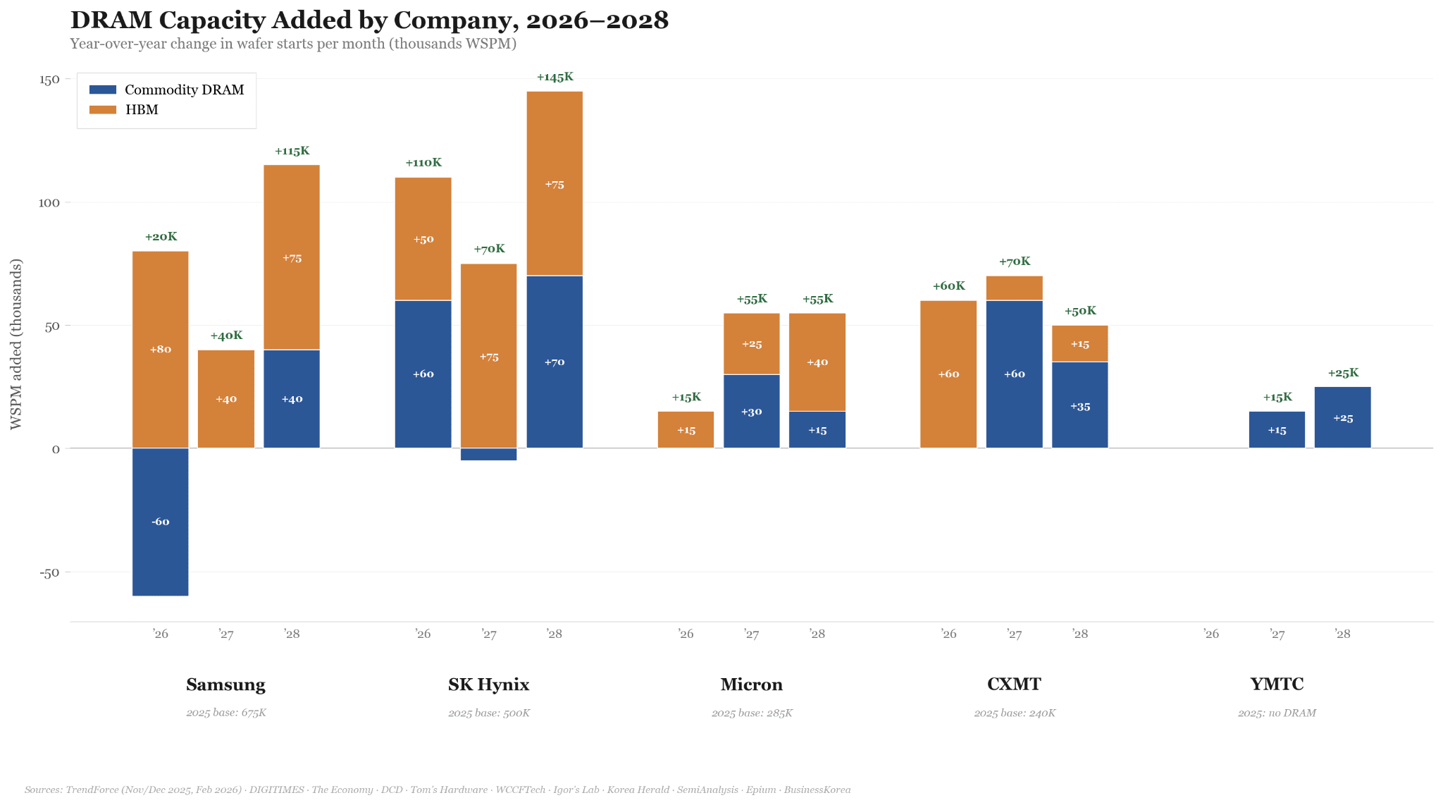
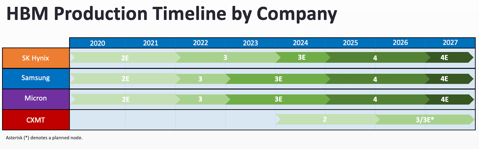
The persistence of the memory shortage also supports the need for alternatives outside of the Big Three (at least until H2 2027). Although everyone is currently spending heavily to expand capacity, fabs take years to come online. Further, as demonstrated below, the demand exceeds supply for HBM too. The capacity that the Big Three is building is for HBM, not for commodity DRAM. So while we wait for the Big Three to have the capacity and incentives to supply both HBM and commodity DRAM, CXMT can fill in the gap.

This situation is not hypothetical. Samsung’s planned memory expansions in its P4 fab and greenfield P5 fab are destined for HBM, not commodity DRAM, so such expansions will likely not alleviate the memory crunch. The story is similar for SK Hynix and Micron. Further, much of what “commodity” DRAM is manufactured by the Big Three may actually go toward AI applications, given server DDR5’s usage in the prefill phase for AI inference. By contrast, CXMT’s ramping production in its Shanghai megafab will be predominantly focused on commodity DRAM, not HBM or products for AI applications.

Made with ClaudeCode. Samsung’s decrease in commodity capacity reflects node migration and increased wafer allocation to HBM.

It is worth noting that the Big Three’s capacity allocation and expansion can play out in one of two ways: either they largely stick to their planned HBM roadmap, or they pivot to shift more allocation toward commodity DRAM. In the former situation, CXMT plays a helpful role moderating the market, pacifying the consumer economy until the Big Three have enough capacity in 2028. This scenario opens up greater risks of market dependency, which are explored in the case against Chinese memory below.

The latter scenario, while possible, is unlikely. Shifting allocation from HBM to commodity DRAM is not at all difficult; one just needs to swap out the masks in front-end fabrication, but all the equipment is the same. Shifting from normal DRAM to HBM is the more difficult transition, though, given HBM’s unique back-end processes. In this light, it makes sense that the Big Three’s expansions are all nominally targeted for HBM, as doing so gives them flexibility. However, shifting from HBM to commodity DRAM carries its own risks. By switching to commodity, fabs would effectively be losing money by underutilizing the tools that should have been used for HBM’s back-end processes. For semiconductor fabrication, where unit economics is king, downtime on tools is a cardinal sin.

However, some commodity DRAM products’ profit margins are superior to HBM3E, so perhaps more companies will dedicate more capacity as their HBM contracts are fulfilled. But anyone who says they know how the allocation will shake out is lying. Companies have some incentive to persist in HBM production even in the face of better commodity margins, as AI demand is more stable than the cyclical commodity market. Over the long-run, HBM yields better profit margins, even if DRAM booms cause the balance to shift temporarily. But perhaps a company will miss out on some HBM contracts or have process issues, making the allocation to commodity DRAM a better route. This is a dynamic process, involving variables ranging from the fate of the global economy, AI progress and developments, contract agreements, and individual business decisions. But if companies allocate more toward commodity DRAM than originally perceived, then the need for CXMT declines, circumventing potential concerns of market dependency.

After 2028, the crisis will likely have passed, and we can return to normal. At this point, the other fabs will have introduced enough capacity to render CXMT obsolete. Projects like SK Hynix’s Yongin megafab and Micron’s Boise and Tongluo fabs will be able to alleviate more of the demand. Further, commodity memory is notorious for being a glut-to-drought cyclical industry. By 2028, no one should be surprised if demand for commodity DRAM or even HBM dries up, causing a crash in prices instead of a continued surge. This is partially why memory makers are so reluctant to invest in commodity DRAM. (The emergence of LTAs and now so-called strategic customer agreements with five-year contracts is intended to lessen this risk, but we will see how much of an impact they have.)

Such cycles are dependent on consumer demand — a fickle variable tied to the global economy — and how important and memory-hungry AI will continue to be. The answer to the latter has been debated ad nauseam, and this piece largely follows Derek Thompson’s assessment of AI: nobody knows anything. Regardless, the odds are that by 2028, customers will not want to turn to CXMT for memory anymore.

Geopolitical Advantages

Another line of reasoning suggests that allowing Chinese memory into the American market may actually further our national security interests. By giving CXMT access to a lucrative market for their DRAM, they may be less incentivized to invest in HBM. After all, HBM would be a high-risk venture with certainly low yields (and thus, lower margins) in its early days.

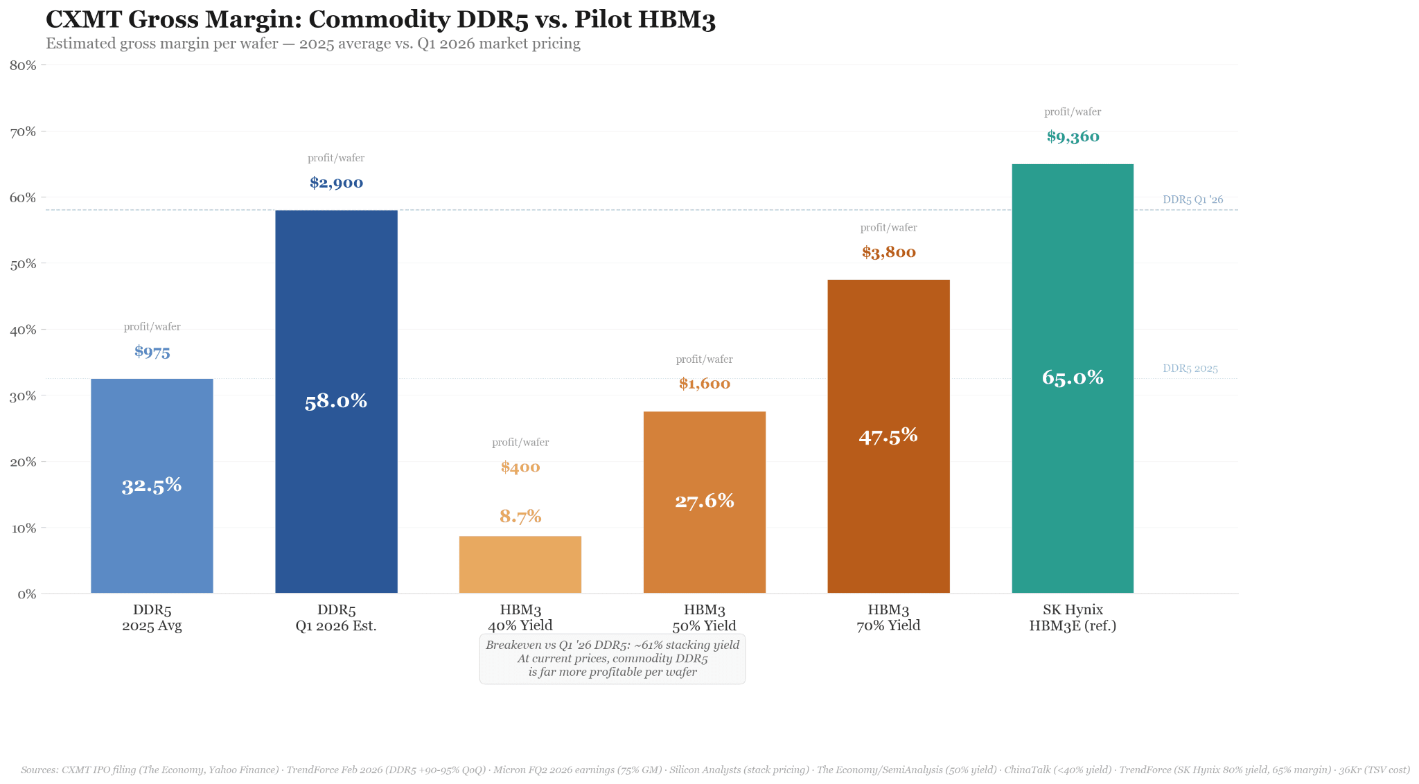
CXMT is expected to dedicate 20% of its increasing capacity to producing HBM3 this year, but perhaps it can be incentivized to move away from the AI market. Already, commodity DDR5 margins are exceeding profits from HBM3E among the Big Three. Considering that HBM3E is already achieving mature yields, imagine the incredible profit comparison for CXMT’s DDR5 versus a pilot HBM3 it has yet to start. Rough estimates indicate that a TSV yield of near 60% is the inflection point where HBM becomes more profitable than commodity DRAM, and a yield of upwards of 70% is required for the margin percentage to be better. However, given some estimates that CXMT won’t break 40% until the end of 2026, CXMT seems to be a far cry from reaching that inflection point.2

Made with ClaudeCode.

Given the importance of AI to Chinese customers and governmental actors, it is ludicrous to think that CXMT will give up HBM altogether; after all, the company may be able to realize a better profit on HBM over the long run if it increases yield and finds a way to keep progressing (an uncertain prospect). This is the same logic the Big Three are currently following. However, in the short run, bales of cash may induce CXMT to temporarily prefer commodity DRAM over its HBM ambitions. CXMT is not exactly like other Chinese chip companies (like Innoscience) that can run large deficits without care for revenue. Building DRAM and HBM is expensive on orders of magnitude greater than that of compound semiconductors or mature-node chips. Capital matters, and CXMT knows it. Thus, instead of a 20% allocation to HBM, CXMT could be tempted to lower that number to something like 15%. That would be a win.

It would be truly a difficult decision for CXMT to make. CXMT DRAM would be a competitive product internationally, allowing the company to grow more rapidly and have greater market penetration. HBM, while deemed a critical product, would have no global market; the rest of the world is already on HBM4E, whereas CXMT is stuck two generations behind. CXMT’s HBM would be for domestic markets only, and CXMT would have to perform a balancing act between domestic mandates and international growth.

This argument is not certain, however, and prompts objections that CXMT earning more in commodity DRAM can actually support their HBM ambitions; more cash translates to more resources for HBM development and process perfection. This argument is explored in the succeeding sections.

Splitting capacity between American and Chinese customers also causes negative externalities for other parts of China’s AI industry, such as SMIC and consumer-facing companies. Every chip going to an American customer is one not going to a Chinese customer. China’s leading chipmaker SMIC has already announced that its own orders are lagging; because customers don’t think they can secure enough memory chips for a finished product, they don’t bother ordering with SMIC for the logic chip. Further capacity allocated to American industry exacerbates this trend for the Chinese industry. If one believes that the U.S. buying CXMT DRAM supports their HBM ambitions, then by this logic, it would also hurt SMIC’s advanced node ambitions. With fewer orders, they would have fewer resources to develop past 5 nm.

Although a slowdown in the Chinese economy is not inherently an advantage for the U.S., the fewer dollars dedicated to SMIC’s advanced-node developments and Huawei’s AI processors are in America’s interest. Of course, it is again unclear how much capacity American customers would receive, and the Chinese government would certainly clamp down on attempts to leave Chinese companies empty-handed while American companies receive whatever they want. However, the allocation would likely be greater than zero, and the increased tension between the company and the government can only serve American interests.

The Case Against Chinese Memory

Market Dependency

The leading argument against allowing unfettered Chinese memory is predicated on real concerns of market dependency. The U.S. has taken pains to reduce its economic dependence on China for critical industries like rare earths, semiconductors, telecommunication infrastructure, etc. Why would we now allow that dependence to again fester in the form of memory chips?

Even if CXMT does not dominate the American market in the beginning, the company’s foothold in the American market has the potential to skyrocket. No one can serve demand right now, and everyone is attempting to expand capacity. As demonstrated in the previous sections, CXMT will be the first to significantly expand capacity for commodity DRAM. Could this not lead to a long-term, increasing dependence on CXMT? Although the immediate term may lead to helpful bargaining power without real allocation, the future may lead to real allocation that causes genuine entanglement.

It is possible that the Big Three become increasingly “HBM-first” companies, allowing CXMT (and later, YMTC) to take up a bigger share of the commodity market. The trends in wafer allocation could support this claim. The revenue that CXMT generates from this increased market share could be reinvested into R&D, capacity expansion, and even advancement in HBM.

However, it is highly unlikely that Chinese memory companies will play a role larger than end uses constrained to low-performance applications and/or in foreign markets. First, the Big Three will always make commodity DRAM. Large-scale production of DRAM dies helps the companies improve their yield for newer nodes, which are to be used later for HBM. The commodity DRAM is always the first step of the HBM process; they cannot be separated.

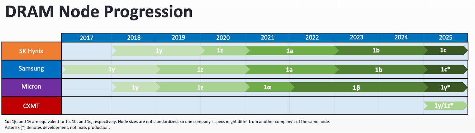
Second, customers will always want commodity DRAM from the Big Three, such that the economics will always tilt toward the Big Three maintaining some amount of commodity DRAM production. The Big Three’s DRAM nodes and performance are leagues ahead of CXMT’s. The Big Three are perfecting their 1c/1γ nodes while CXMT is still on 1y/1z, at least three generations behind. Even significantly cheaper CXMT DRAM is not so attractive given the use cases for memory in consumer products. Apple does not release a new generation iPhone with worse memory, even if it is much cheaper. The same goes for XBOXs and PCs; while some focus on the lower-cost market, the bifurcation of markets for low-cost and high-cost products can only serve consumer interest.

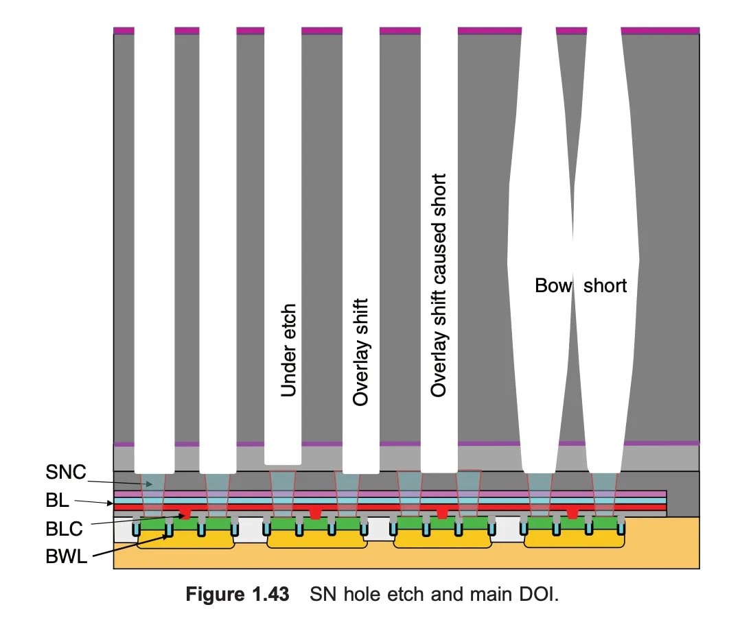
Betting on CXMT not to catch up or plateau is not a bet against Chinese innovation (a poor bet indeed), but rather a bet that export controls on EUV lithography and equipment required for DRAM advancements are effective. China’s domestic EUV capabilities will likely not be realized until 2030 at the earliest, and restrictions on EUV lithography have been an enduring American policy throughout both Republican and Democratic administrations. The $400 million machines are colossal and monopolized by ASML, meaning smuggling is not as serious an issue as it may be for individual chips.

Export controls condemn CXMT to only applications that do not require cutting-edge memory. That is an important market segment, but nothing near an impending monopoly or concerning supply chain risk. And even in these segments, other companies like Taiwan’s Winbond and Nanya will have room to compete and prevent a Chinese monopoly.

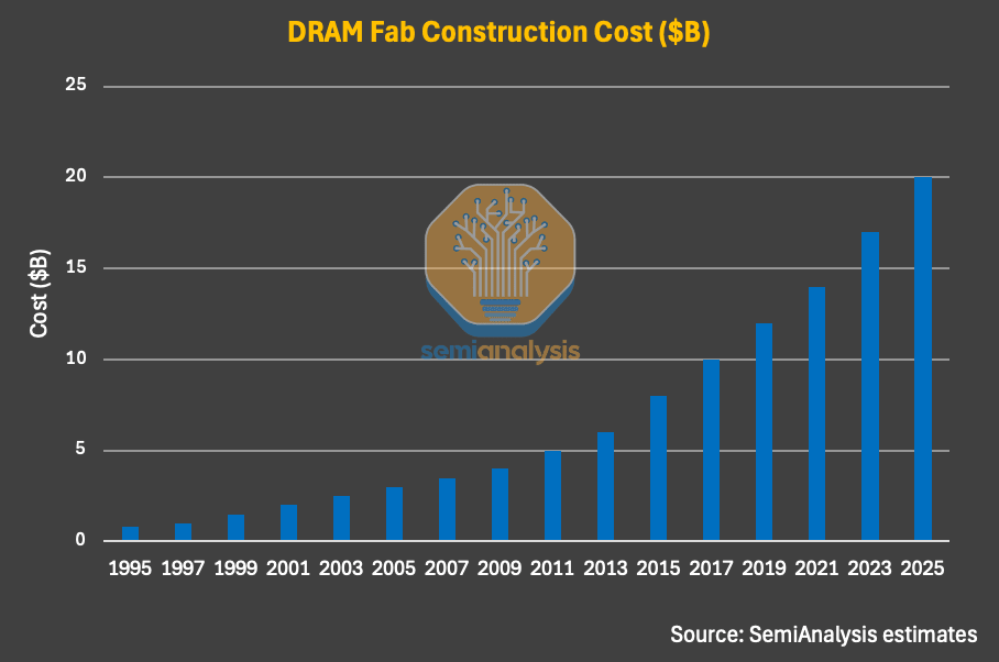
Lastly, this world would cause CXMT to constantly be tugged away from allocating more capacity toward HBM. Although revenue generated from the commodity segment may help CXMT build more and research better, they will be faced with tough decisions in wafer allocation. The market disincentivizes companies from building enough capacity to perfectly satisfy both commodity and HBM demand, as no one wants to be left holding the bag on a $20 billion fab once the cycle declines or if the AI bubble bursts.

Cautious expansion is the philosophy for everyone in the chipmaking space, for reasons well explained by Asianometry with respect to TSMC, the bullwhip effect, and the beer game. In brief, small variations in demand from retail consumers or AI players cause the greatest volatility for the suppliers at the end of the chain. If everyone in the world starts buying one more candy bar from the gas station, the gas stations feel it slightly, but the candy bar factory gets slammed the most with orders. If everyone starts buying one fewer candy bar, then the gas station barely feels it, but the candy bar factory can go broke. When the memory industry inevitably experiences a demand downturn — no matter how small — the memory makers will suffer the brunt of the fallout.3

Geopolitical Disadvantages

The stronger argument against Chinese memory is a geopolitical one. Every dollar going to CXMT and YMTC, regardless of how it benefits the American economy, would also be benefiting companies widely considered national security risks.

Although American policymakers have a tendency to think that Chinese companies have open checkbooks from the Chinese government, they need a great deal of supplemental funding to support their ambitions. CXMT’s recent IPO (and YMTC’s impending one) demonstrates the need for billions of dollars more capital to fund capacity expansions and R&D. American companies giving CXMT money for DRAM, thus, is America funding China’s HBM ambitions.

Source: SemiAnalysis

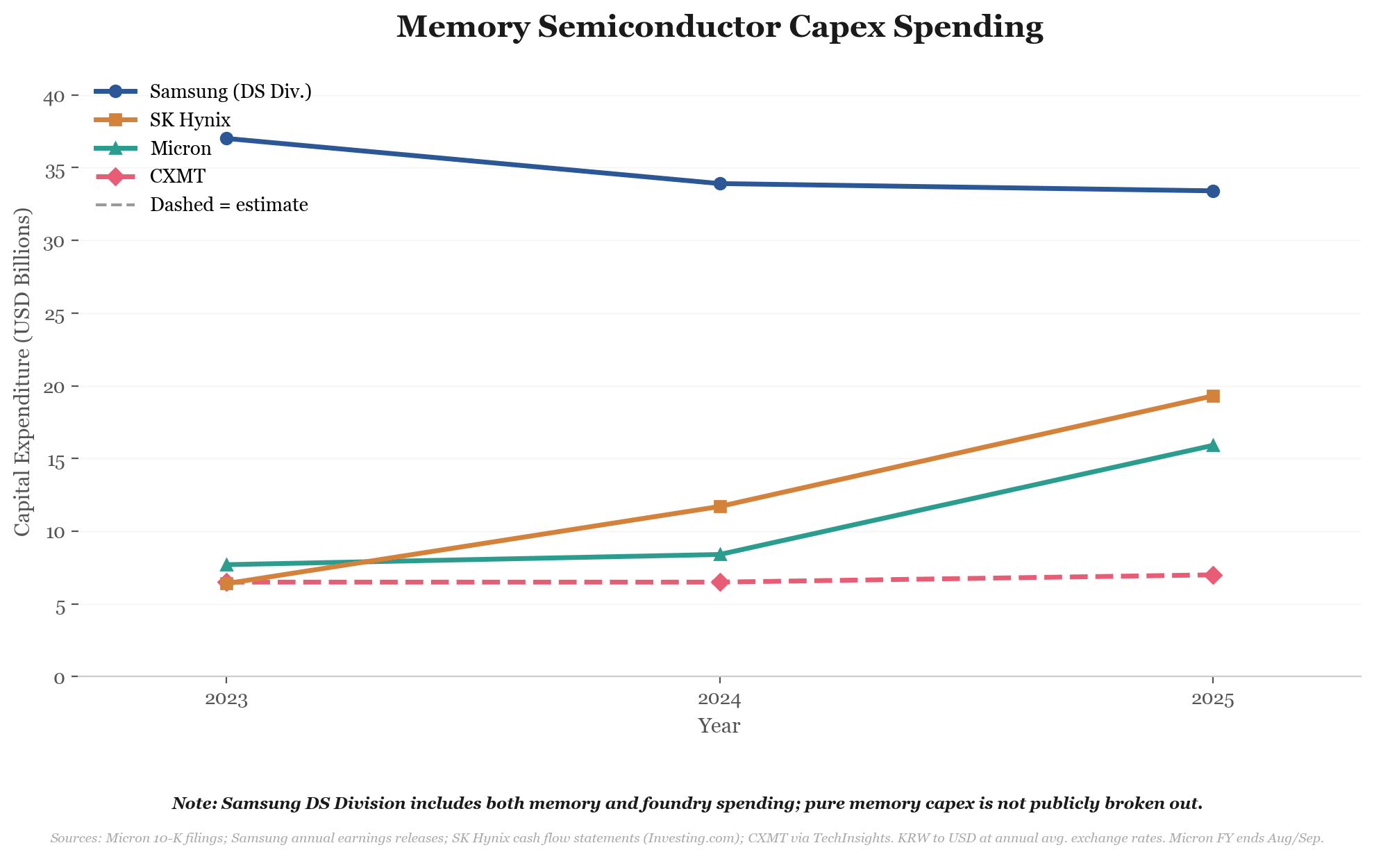
One of the Big Three’s biggest advantages currently is their ability to spend on capex in a way that CXMT cannot. These dollar amounts go toward node migration and capacity expansion — the reasons we’re ahead right now. Perhaps allowing CXMT to proliferate in the market will reverse this advantage.

Made with ClaudeCode.

Another concern is the reality that American customers would be helping to perfect CXMT’s processes by qualifying them as a supplier. For example, if Apple desires to qualify CXMT for its LPDDR5X in iPhones, then Apple will work with CXMT to make its processes more reliable and better performing. Apple engineers would literally assist CXMT’s products to outperform the JEDEC standard and meet rigorous requirements for metrics like thermal performance and consistency. Do we want American engineers helping Chinese companies in this way? It’s a hard pill to swallow. These technological advancements directly translate into CXMT building better HBM for AI demand.

And once qualified, ecosystem stickiness poses a problem. Even if the Big Three have capacity available once again, companies will have already gone through the trouble of qualifying CXMT as a supplier. Why not stick with them as a significant supplier, specifically for low-cost applications or in markets where price matters more than performance? How this plays out is again impossible to predict, but believing that CXMT will remain a major player beyond this memory crisis is a real possibility.

Aqib’s Verdict

Ultimately, the risks associated with permitting CXMT market access are grounded in more exaggerated doomsday scenarios rather than rigorous analysis. Giving CXMT money and qualifying it sounds scary, but the downsides seem to pale in comparison to the benefits. We shouldn’t care more about making sure China stays inside a box than the welfare of American citizens.
The fear of CXMT represents a prevailing American paranoia of anything associated with the five-star red flag. China is an adversary, but each decision should be predicated on rigorous cost-benefit analysis, not blanket anathema. Buying from CXMT will certainly help them in some way, with increased funding and a level of technological progress, but this is a far cry from China catching up or posing a threat.

First, CXMT’s progress will be more stymied by American export controls than benefited by customer revenue. Cracking future nodes of DRAM is more a technical problem than a financial one. Second, the technological benefits from being qualified by American customers should not be overstated. CXMT is already qualified by major players like Chinese smartphone, PC, and cloud computing companies. These companies already push CXMT to progress beyond industry-required minimums. An Apple partnership will perhaps move the needle a bit, but it is not like the U.S. would be helping them discover fire.

The ecosystem stickiness argument is the most defensible, but this piece does not weigh it as heavily compared to the myriad benefits. The Big Three produce better memory compared to CXMT on a performance basis, mainly due to the yield superiority gained from technological advancement and export controls. By 2028, just like 2026, CXMT will not be in the same league as the Big Three in terms of memory quality. Without advanced tooling, they cannot reach yields or performance specifications like the Big Three can.

The semiconductor industry is unlike electric vehicles or solar panels. Although China may offer cheaper products, the risk of market dependence is not so serious. Export controls and the difficult science of semiconductor manufacturing indicate that CXMT will be behind for years. The current market crunch is not a permanent state of affairs by any evaluation, but rather a temporary pain that requires a temporary solution. The players in the industry are also not engaged in a race to the bottom that China will win, but rather a race to the next node that China will lose.

The options are also not binary. The U.S. can permit CXMT now, when the benefits are attributed more toward bargaining power than to actual capacity allocation, and slam the door later. Other policy options to reap the benefits while managing the downsides exist, including greater tariff impositions, requirements on customer allocation ratios, etc.

Permitting now but slamming the door on Chinese memory later can also have added benefits. If CXMT expands capacity to satisfy American demand now, being shut out later would leave the company holding the debt of underutilized fabs and equipment. Of course, this is a severe oversimplification, and CXMT is not this dumb, but the regulatory uncertainty adds a layer of benefit.

Perhaps the best means of managing the benefits and downsides of permitting Chinese memory is allowing it in limited contexts. If the U.S. permits American companies to qualify CXMT solely for products destined for the Chinese market, then the scope of the “exposed” market is narrowed. For example, only iPhones for the Chinese market could contain Chinese memory, and the overall savings may be distributed throughout the market worldwide. However, this policy option, in my view, is worse than the aforementioned ones.

Banning CXMT is the least defensible policy position right now. The memory crunch is here, but it is not here to stay. Let’s allow the market to do what it will in the interests of our own people. Seeing ghosts in national security threats here discredits real national security threats elsewhere, so let informed policy reign, and let the DRAM flow.

1

Samsung’s DRAM capacity is between 650,000 to 700,000 wpm. SK Hynix’s is 500,000 wpm. Micron’s is between 340,000 to 500,000 wpm. CXMT’s is 300,000 wpm. After accounting for capacity allocated to HBM (about 40% for Big Three and 20% for CXMT), Big Three have an aggregate of 957,000 wpm for commodity DRAM whereas CXMT has 240,000 wpm. These numbers are estimates and intended to represent the capacity of CXMT compared to the Big Three.

2

This estimate of 40% should be taken with a grain of salt, as it results from the ever churning semiconductor rumor mill. The estimate also suggests CXMT will use MR-MUF for stacking, which while widely theorized, has not been confirmed.

3

This also suggests that one way to incentivize the Big Three to expand commodity capacity is via memory customer behavior. If memory customers like Apple form longer-term agreements with memory makers, agreeing to regularly purchase memory for X amount of years, memorymakers will be more incentivized to expand capacity. In this case, they know they won’t be left holding the bill if a drought occurs. This level of LTA is unprecedented in the memory industry, but longer term agreements are emerging. Further, this would result in memory customers holding unusual risk that may collapse firms in the event of a demand drought.

How Much Compute Does China Have?

How much compute does China have? Despite its all-important relevance to American export controls, the AI race between the U.S. and China, and national security, this question remains unanswered.

Today and tomorrow, ChinaTalk will attempt to answer the question using two very different methods. Today’s article attempts to estimate China’s compute via a bottom-up (supply-side) approach. This piece will try to brute-force count every chip procured through every possible means. Tomorrow’s article by Nick Corvino attempts a demand-side approach. That piece tries to deduce the amount of compute China has based on the needs of training and serving the country’s models. The two articles, hopefully, provide a solid range of estimates that inform policymakers, but also future researchers attempting to understand China’s compute supply.

The work for the two articles was conducted independently, and only after completion did we compare notes. Surprisingly, despite large uncertainties on both sides, we arrived at nearly the same number! Both estimates were roughly 2.8 million H100e, and the convergence of estimates suggests we may be on the right track.

A disappointing disclaimer: the answer is unknowable for any tight ranges. Although both pieces get to a number — one that we are confident is correct within an order of magnitude — we would be shocked if it were accurate far beyond that. The biggest reasons for high variability on the supply-side are twofold: lack of understanding how much compute China accesses remotely, and the inherent opaqueness of chip smuggling operations.

Ultimately, this analysis should not have required this much guesswork. Without a concrete answer, the success of our export control regime and national security framework, as well as our perceptions of our advantages against China, can only be based on hunches. A credible number is needed to understand how well export controls are working, to what extent we are ahead of China, and to track China’s behavior.

Such high variability in this estimate should inspire the U.S. government to adopt mechanisms that enable us to monitor our adversary. These mechanisms include the ability to peer into the operations of hyperscalers, neoclouds, and all forms of cloud-service providers (CSPs). Even if not to obstruct their operations, the U.S. government cannot know how China is using and abusing compute without this information. A Know Your Customer scheme or something similar is required to enforce the policies we have already implemented and to know how they are being circumvented. We hope that the U.S. secretly maintains a credible estimate via aforementioned methods or other channels; however, in the case that this work is not redundant, it will serve as an important tool for policymakers and China Hands alike.

For maintaining standardization across chip generations, this piece quantifies compute as “H100-equivalents,” or H100e. H100e is measured by dividing the peak operations per second of a chip at FP8/INT8 by the H100’s specification. This is the method used by Epoch AI. It is important to note that simply calculating FLOPS does not give the whole story of a chip; elements like memory bandwidth, memory capacity, and software are critical for a chip’s performance and usability. Until we have something better, though, FLOPS are what we have and what we will use.

Bottom-Up (Supply-Side) Calculation

From a supply-side calculation, China’s compute can be understood as the number of chips within China plus the number of chips China can remotely access abroad. The former category can be further broken down as the number of chips China has legally purchased from abroad plus the number of chips China has illegally purchased from abroad (smuggled chips) plus the number of chips China has produced domestically.

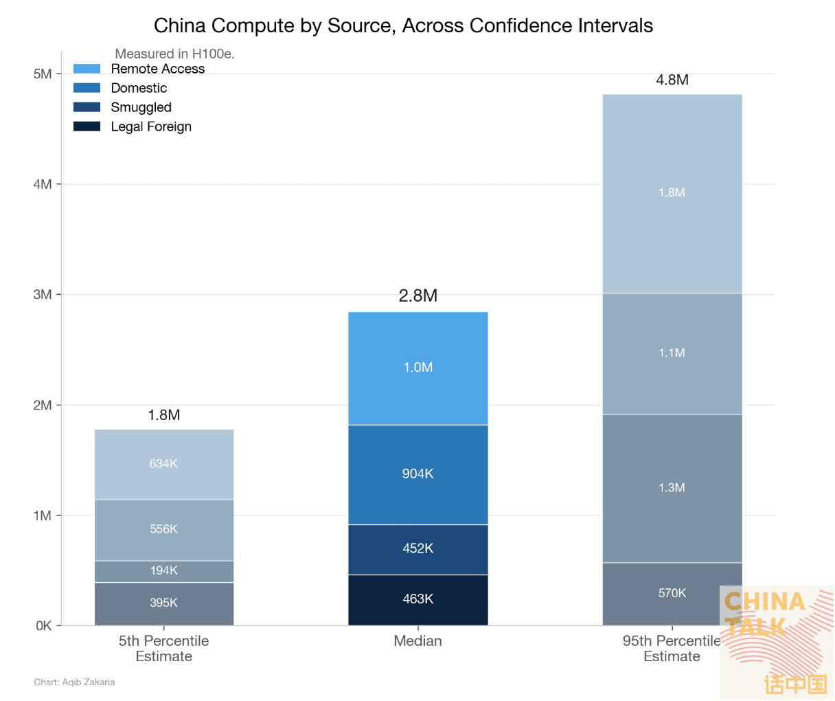
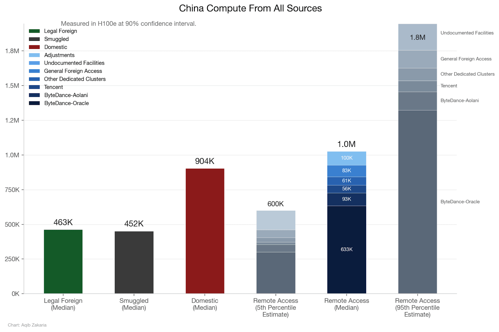
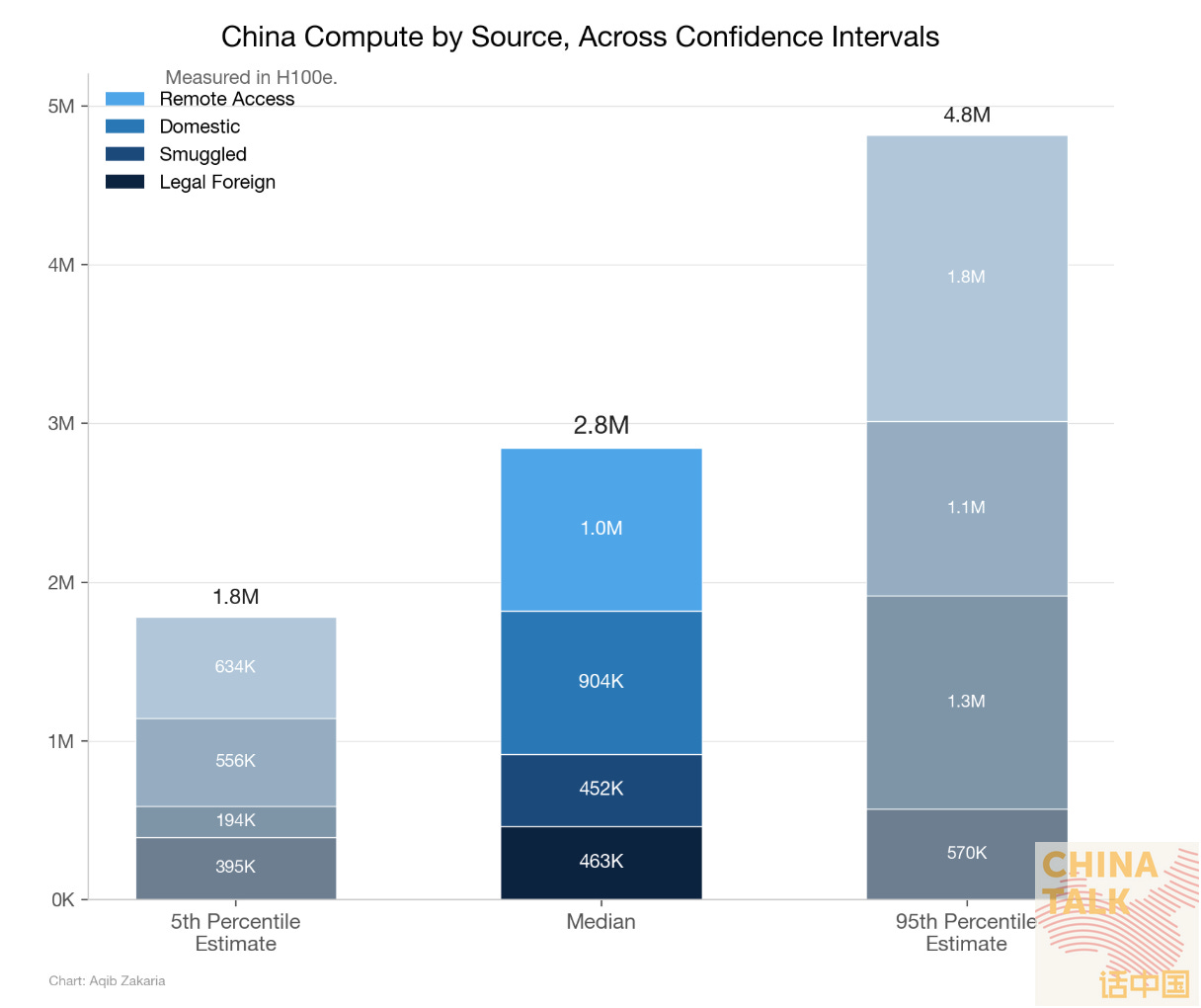
From this calculation method, this piece approximates China’s compute supply to be about 2.8 million H100e, with 90% confidence in a range of 1.8 million H100e to 4.8 million H100e. The bulk of this comes from compute from domestic companies and compute remotely accessed via the cloud, but both legal purchases from foreign vendors and smuggled chips play a non-negligible role.

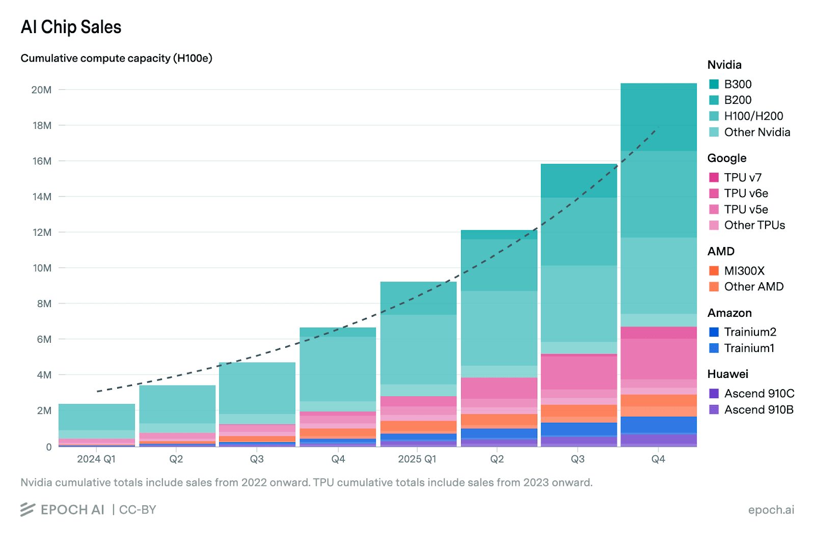
For context, Epoch AI estimates the cumulative compute by leading chip designers to total 20 million H100e. This suggests that China has access to about an eighth of the world’s compute.

Legal Foreign Compute

Starting with foreign, legally purchased chips, China has placed its largest orders with Nvidia and, to a lesser degree, AMD. Other specialized chips, like TPUs and AWS Trainiums, have typically been tied to specific hyperscalers or platforms and, thus, nonexistent on Chinese soil. Intel’s Gaudi line, while not specialized, was a commercial failure with no confirmed Chinese buyers.

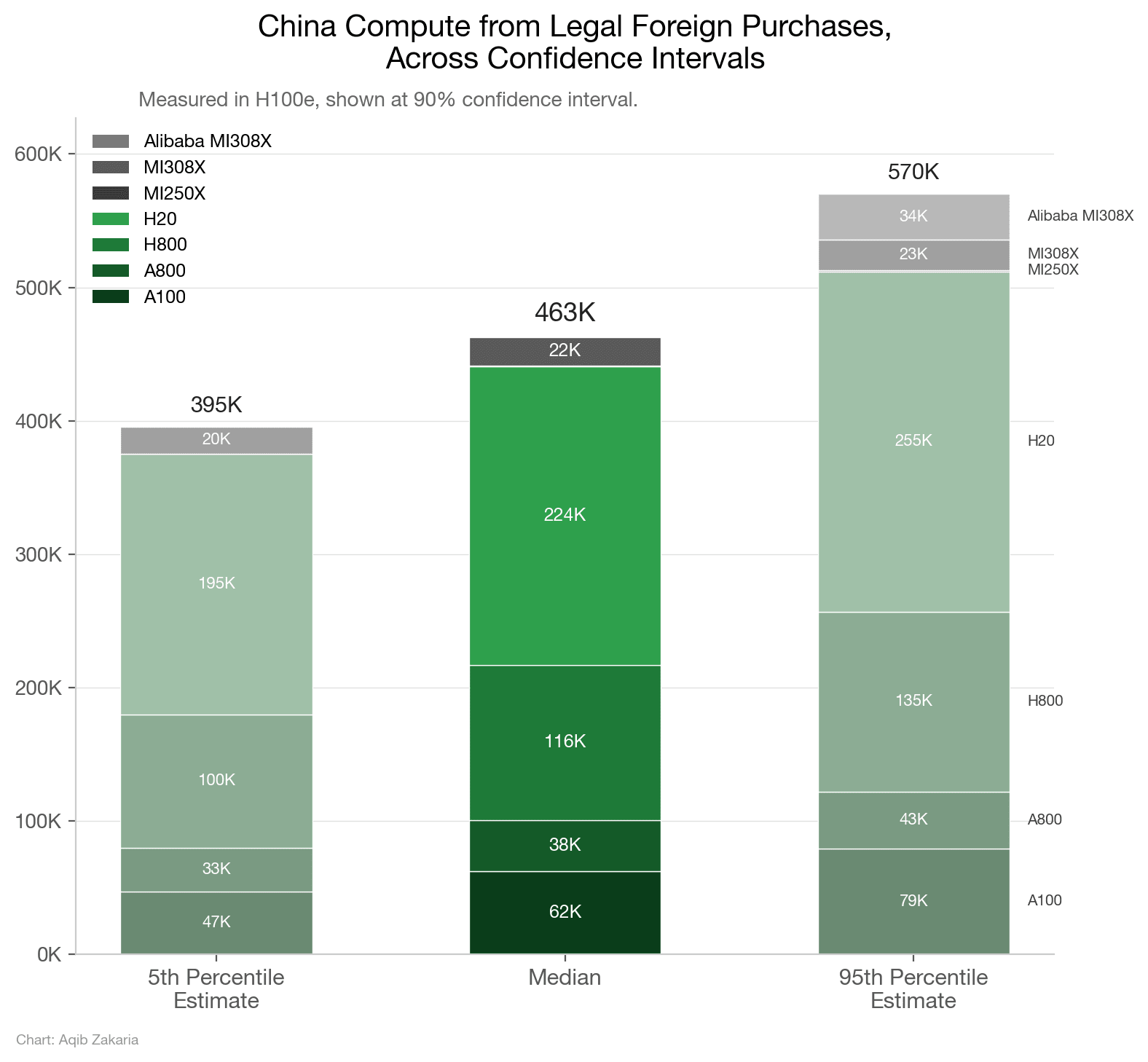
Prior to BIS’s October 2022 export controls, Nvidia’s A100 — released in 2020 — was legal for purchase. During that two-year period, China likely purchased around 197,789 A100s (62,363 H100e). Similarly, China likely purchased roughly 3,000 MI250Xs (582 H100e), the AMD equivalent of the A100. These numbers have the loosest confidence intervals, as A100s and MI250Xs were destined for the global market and estimating the breakdown of distribution to China is an imprecise science. However, the legal Nvidia sales of models after the A100 were for China-specific designs, giving us greater confidence. The numbers given reflect EpochAI’s data, which are at a 90% confidence interval.

The October 2022 export controls restricted the sales of A100s and other AI chips based on the criteria of network bandwidth and arithmetic performance. To circumvent these restrictions, Nvidia produced the A800 and H800 for the Chinese market. These chips, roughly equivalent to the A100 and the H100 in arithmetic performance, were made with downgraded network bandwidth so as not to be restricted. BIS revised its export controls to restrict the A800 and H800 in October 2023, but during this one-year period, Chinese customers were able to procure roughly 121,077 A800s (38,175 H100e) and 116,423 H800s (the same in H100e).

After October 2023, the regulations on arithmetic power were far stricter, so Nvidia developed the H20 for the Chinese market. The H20 possessed about 15% of the arithmetic power of its contemporary H200, though the chip was designed with outsized memory bandwidth capabilities, making it ideal for AI inference applications. The H20 indicates the shortcomings of the H100e methodology: despite its low performance in H100e terms (a unit better designed for measuring training strength), the H20 is arguably more powerful than the H100 for serving inference. Regardless, the H20 was sold until April 2025, during which China likely purchased 1,495,352 H20s (223,658 H100e). During that same period, AMD’s equivalent of the H20, the Instinct MI308X, was produced but sold in much smaller quantities. To date, Epoch AI estimates that Chinese buyers have purchased 32,500 Instinct MI308X (21,523 H100e).

In all, legal purchases from foreign providers account for over 460,000 H100e, with a 90% confidence in a range of 395,000 H100e and 570,000 H100e. The range is predominantly due to the uncertainty on A100 sales, but the full error bar analysis is here. These legal purchase calculations do not include pending orders for Nvidia’s H200 and AMD’s MI325X, as these orders have yet to be confirmed and seem to be in regulatory limbo. It also does not include Alibaba’s pending order for the MI308X, though this is accounted for in error bars. Processing such orders could drastically enlarge this total, depending on the quantities allowed to Chinese customers. Of all the categories of compute we estimated, legally purchased compute from foreign companies is the calculation we have the most confidence in. The companies selling compute to China are all public, and gleaning Chinese compute purchases from their filings is relatively easy compared to subsequent calculations.

Smuggled Compute

Besides legal purchases of foreign chips, some amount of China’s compute comes from chips illegally smuggled into the country. These are usually high-power chips restricted by export controls, such as Nvidia’s H100, H200, and newer B200.

Until the end of 2023, China had legal access to powerful Nvidia chips. Even the A800 and H800 were barely downgraded compared to their originals, but were legal due to poor export control design. Thus, important amounts of smuggled chips likely accumulated beginning in 2024.

CNAS reports a median estimate of 140,000 chips smuggled into China for 2024, with 90% confidence in a range of about 17,500 chips to 780,000; because actors are incentivized to smuggle the best chips — not legal ones or generations that are just not worth the effort — 2024 chips are considered to be predominantly H100 and H200s. The Blackwell series was not being shipped until the very end of 2024. Thus, roughly 140,000 H100e were smuggled into China in 2024.

In 2025, the amount of compute smuggled into China was likely larger than in 2024, due to two factors: increased power of chips and greater need. The Blackwell series was being shipped in large quantities throughout 2025, and the B200 has approximately 2.5 times the performance of an H100, according to Epoch AI. The Financial Times reported that at least $1 billion worth of Nvidia chips were smuggled into China in one quarter of 2025, with the B200 being the most popular and available offering.

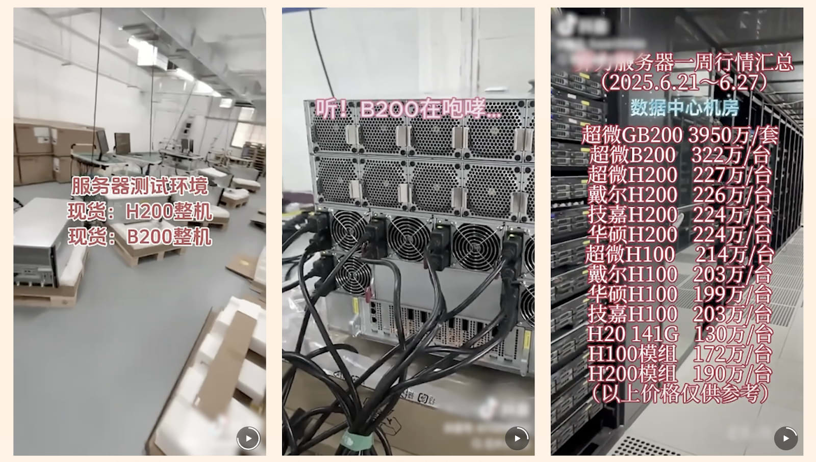
Videos from Chinese social media demonstrating smuggled Nvidia chips being tested and sold. Screenshot from the Financial Times.

Also, after the H20 was banned in the middle of 2025, Chinese firms had a greater incentive to smuggle chips. While the H20 provided an ample supply of inference compute, its restriction caused a need for Chinese customers to acquire their compute elsewhere — some of which was likely via smuggling.

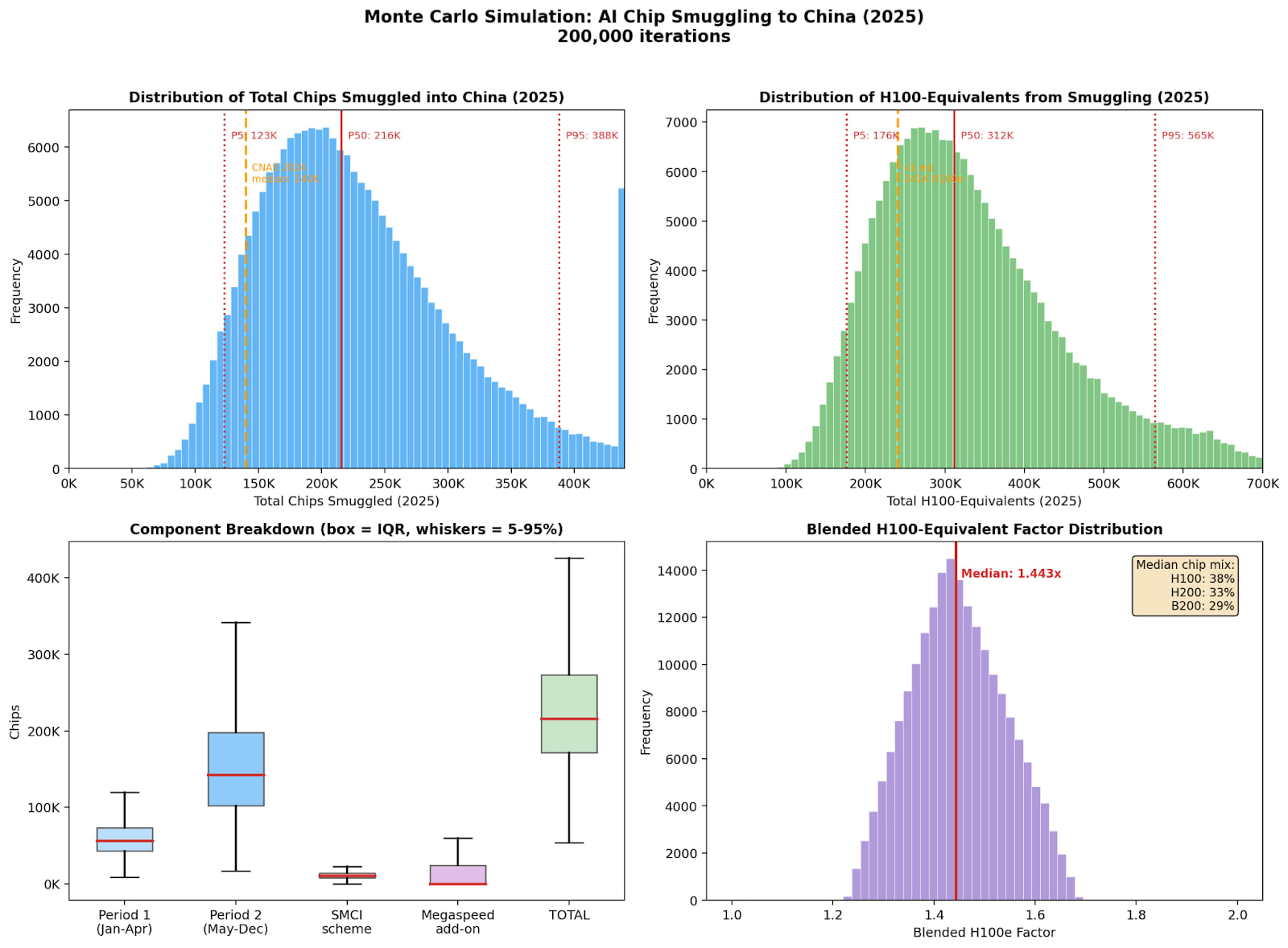
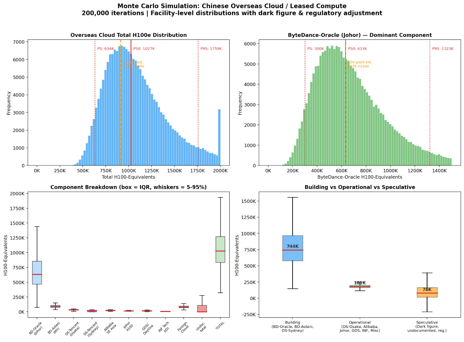
I ran a Monte Carlo simulation (repo here) similar to the one conducted by CNAS in its 2024 estimate, and the results suggest a median of 312,000 H100e were smuggled into China in 2025, with a 90% confidence in a range of 176,000 to 565,000. The results are most definitely not to be taken as gospel, though they attempt to account for the impact of the H20 ban, the emergence of the Blackwell, and reported instances of smuggling like the Financial Times’s report. As a testament to the high variability of this estimate, the recent news of the plot by Supermicro executives to sell $2.6 billion worth of Nvidia chips to China drastically changed the calculation. The simulation estimated a median of 240,000 H100e prior to this news, demonstrating that every new data point can wildly alter the estimate. After the Supermicro news, the lower bound of smuggling was increased, driving the median up to 312,000.

Monte Carlo simulations involve assigning probability distributions to different inputs based on evidence and reports. The simulation rolls a dice 200,000 times randomly picking values for the inputs within their distributions and then tallying the results. What we get is shown below, with a range of possibilities and a somewhat-educated range. It’s high variability and requires many assumptions, but it is the best we have.

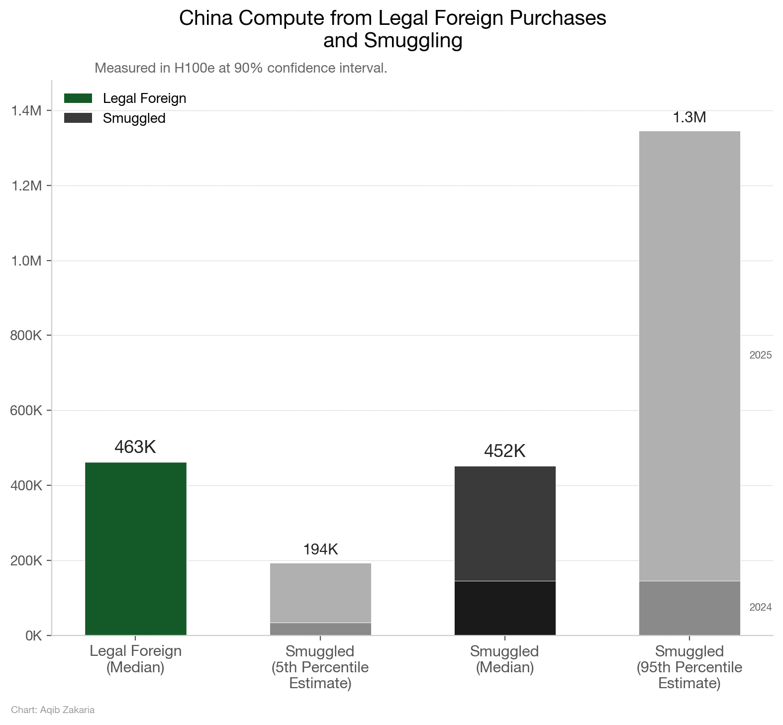
The sum of Chinese compute smuggled into the country is likely in the ballpark of 452,000 H100e, most of which was smuggled in the past two years. The 90% confidence range is between 193,500 H100e and 1,345,000 H100e. It is unclear how usable much of this compute is for large-scale clusters, as Nvidia would not service such clusters if the chips were to run into issues. However, the jury is still out on how easily non-Nvidia engineers can fix potential issues with Nvidia hardware.

This estimate also gives rise to a strange conclusion: China was likely able to illegally import as much compute as they were able to legally import. This can be partially explained by the fact that China’s window for legal purchases was narrower than the window for smuggling in higher-performance chips. Further, demand for AI chips was at its lowest in 2020, when the A100 first came on to the market, so the low number of legally acquired chips during that period is understandable.

Homegrown Compute

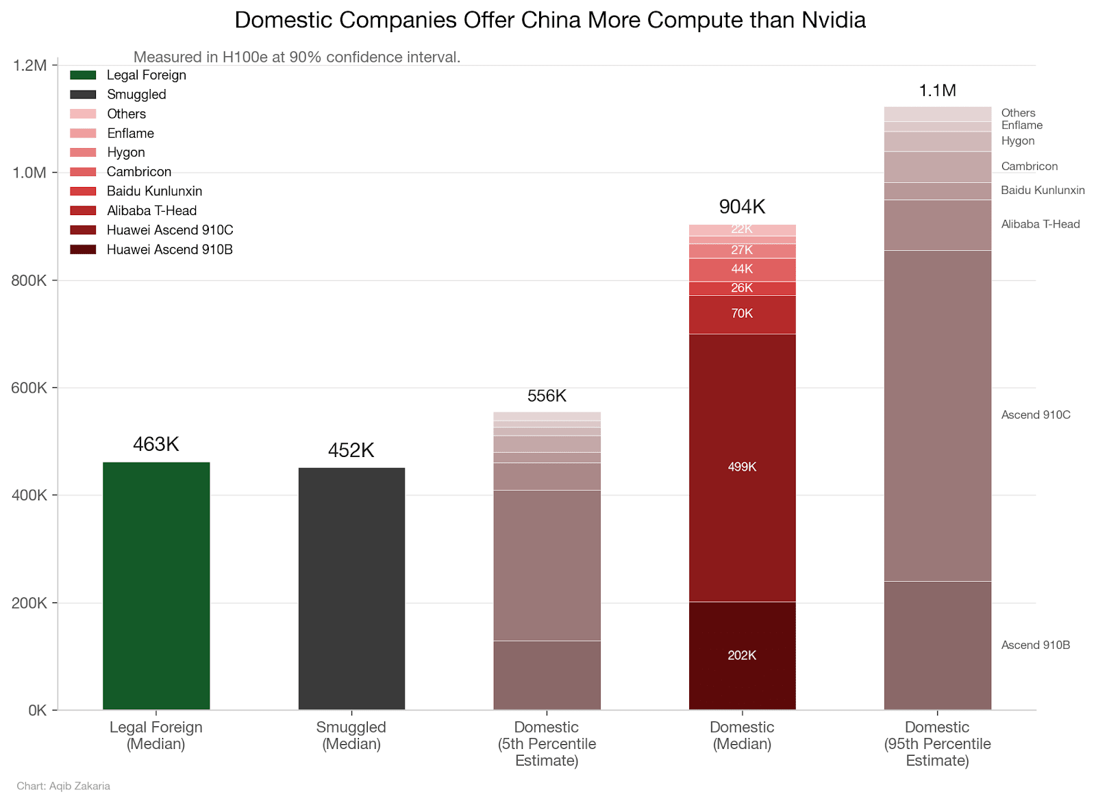
For homegrown compute, China’s champion is Huawei, with its Ascend 910B and Ascend 910C products. Using Epoch AI data, both have been in production since Q1 2024, and China has acquired roughly 600,000 Ascend 910Bs (201,798 H100e) and 650,000 Ascend 910Cs (498,971 H100e).

China also has a competitive AI accelerator industry, which also accounts for a decent chunk of compute. Providers include: Alibaba’s T-Head (平头哥), Baidu’s Kunlunxin (昆仑芯), Cambricon (寒武纪), Hygon (海光信息), Enflame (燧原科技), Moore Threads (摩尔线程), Iluvatar (天数智芯), Biren (壁仞科技), and MetaX (沐曦). Although none individually comes close to Huawei’s scale, some have shipped hundreds of thousands of units, and in the aggregate, they contribute meaningfully to China’s compute supply.

After Huawei, Alibaba’s T-Head is likely the biggest supplier of domestic Chinese compute, with an estimated 470,000 chips (70,500 H100e) sold to date. Next is likely Baidu’s Kunlunxin with an estimated 200,000 chips (25,800 H100e). Then it’s Cambricon with 170,000 chips (~44,030 H100e), followed by Hygon with 160,000 chips (~26,560 H100e).

Other companies have much smaller order numbers. As of 30 June 2025, Iluvatar has shipped roughly 53,000 units (~9,600 H100e) of its AI chips. For roughly the same timeframe, Moore Threads has shipped 25,000 chips (~3,750 H100e), and Enflame has shipped 80,000 chips (~15,000 H100e). Lastly, MetaX and Biren account for 25,000 chips (~6,075 H100e) and 12,000 chips (~2,304 H100e) respectively. Other companies like Tsingmicro and Sunrise are also known to have shipped at least 10,000 units, but specifications on their chips and the actual number of orders are impossible to find.

Omitting the smallest companies (Tsingmicro, Sunrise, and others in their league) with no public specs, the total compute derived from domestic Chinese companies comes to about 904,000 H100e, with 90% confidence in a range of 560,000 H100e and 1,100,000 H100e. The larger range is due to uncertainty of H100e conversion factors for chips, especially Huawei’s, and some uncertainty on exact unit counts. The full analysis of the error bar is included here. This estimate is likely more accurate than the estimates for smuggled chips or remotely accessed compute, as their numbers can be derived directly from company reports. Some of the companies listed also intend to go public in the near future, and their IPO prospectuses could more clearly reveal their revenue streams and shipment volumes. These documents would help us better gauge the amount of compute Chinese companies are actually able to make.

However, there is significantly more uncertainty that Chinese AI chips can actually deliver on their promised specs. Until we get Huawei hardware on ClusterMAX, it’s an open question just how good Huawei’s chips and accompanying software really are.

Remote Access Compute

This estimate is the mother of all uncertainties. Estimating how much compute China can remotely access via the cloud is a gargantuan task, as controls against remote access are weak-to-nonexistent and actors can easily skirt them.

I calculated a total for remote access with another Monte Carlo simulation, which produced a median estimate of roughly 1,026,000 H100e, with high variability. The range for this estimate is between 600,000 and 1,800,000 H100e.

In order to do this calculation, I factored in the range of possible compute at dedicated clusters built by Chinese entities abroad. The biggest variable is the ByteDance-Oracle Johor cluster, and I also included ranges for projects by Tencent and Alibaba throughout Southeast Asia. Some facilities, like INF Tech, have confirmed counts of GPUs, so their range is tightened. I also accounted for similar ranges for American, European, and other Asian data centers, and those ranges were predicated on tender documents and other reports. I also included a range for a multiplier to account for undiscovered compute access. For transparency, in addition to the .py file linked above, the calculation details are included in a .csv file with explanation in an .md file, located here. Further research will almost definitely narrow the range of compute for different projects and data centers, thus tightening the range for the total estimate.

Source: ClaudeCode

More research hours should be dedicated to following the paper trails of companies collaborating on data center buildouts, particularly in Southeast Asia. This is also where mandated reporting of Chinese customers via a KYC scheme or through the enactment of legislation like the Remote Access Security Act could have the most impact. From my own conversations, the extent of Chinese access to neoclouds is the least understood, and also an area where further research can lead to needed information. I have heard many stories of dogged requests by Chinese customers requesting to access neocloud compute: how many neoclouds are accepting the offer, and how much compute does that total? The answer is important and may skew the above estimate greatly.

The size of the median estimate may be shocking to some, as it surpasses the size of compute from all other sources. The projects in Southeast Asia are the largest contributor to this, especially as they contain leading-edge chips which would be far more powerful compared to legally purchased Nvidia chips or indigenous Chinese chips. (See the recent reporting from The Wall Street Journal on ByteDance’s collaboration with Nvidia via Aolani Cloud). These chips may then be remotely accessed by Chinese labs, effectively rendering export controls on such chips impotent. However, the plain number does not properly explicate the compute’s usefulness; due to latency requirements, Chinese actors likely cannot utilize this compute pool for large-scale training purposes.

Final Calculation

Adding it all together, this calculation reached a median estimate of 2.8 million H100e. For context, Epoch AI estimates the cumulative compute by leading chip designers to total 20 million H100e. This suggests that China has access to more than an eighth of the world’s compute; the U.S. would presumably have some level of access to the rest (subtracting the marginal compute used exclusively by non-American labs). Some of China’s compute — the portion able to be remotely accessed — would presumably be accessible to American customers as well.

Source: EpochAI

This calculation simply tallies the number of chips sold to China in recent years and the number of remotely accessible ones. However, the true number may be dramatically different in either direction due to uncertainty in the smuggling and remote access numbers. This estimate also does not take into account the number of chips that have become inoperable after burning out from usage. Having politely asked all four major American cloud providers, unsurprisingly none will give us any color on just what percentage of their compute is serving China-headquartered firms.

To get a better understanding of these numbers would require an act of Congress or the Commerce Department to implement the Know-Your-Customer regulation floated by the Biden administration in January 2024, as well as some mechanism to force Nvidia to tell the government who is using the non-US headquartered neocloud compute in Southeast Asia. Creative policymaking could also create new methods for the government to access CSP customer data without violating privacy rights or exposing CSPs to excessive liability. Brainstorming methods to minimize the governmental invasion of privacy while also securing the information relevant to national security should be a key focus of lawyers and policymakers.

If you liked my attempt at a bottom-up calculation, be sure to tune in tomorrow for Nick Corvino’s article estimating from the other direction.

ChinaTalk is a reader-supported publication. To receive new posts and support our work, consider becoming a free or paid subscriber.

How Much AI Does $1 Get You in China vs America?

The AI race between the U.S. and China will be decided in datacenters.

But who has the advantage? Does the recent H200 ban lift change anything? Many pieces relate vague vibes that the U.S. has better semiconductors while China has cheaper electricity, but they lack numbers. This piece tries to estimate how expensive a data center is in the U.S. versus China, and how much “AI” each data center would generate. This piece does not address Chinese access to chips in Malaysia or through smuggling, a phenomenon that potentially increases China’s access to compute drastically.

BLUF: The U.S. can build much more cost-efficient data centers compared to China, but unfettered access to the H200 would make the race in raw performance extremely close. Access to the H200 gives China a massive boost considering its domestic hardware production constraints. Lastly, the cost efficiency of these data centers is extremely sensitive to the costs of hardware, which is highly variable and not publicly disclosed.

Nearly all of the cost differential comes from two factors: construction and hardware. Other costs, including commonly covered topics like electricity and water, are essentially rounding errors. As such, the main article only covers those two bills, but calculations for everything else are included in the appendix. Because these calculations require some assumptions, I vibe-coded a website that allows you to play with my assumptions and see how the numbers change.

We Run the Numbers

For simplicity’s sake, I will estimate the cost of constructing and operating a 400MW data center over three years. Microsoft’s 400MW Fairwater 1 in Wisconsin is currently the largest AI data center by MW and has decent public information about it, so I’ll take that as our benchmark. I will also limit the operating timeline to three years because data center GPUs often have lifespans for only that long.1 I’ll run through the calculations below, with exact numbers and calculations in footnotes.

Construction

Constructing a data center takes an enormous amount of capital. The plots can be enormous, as demonstrated by China Telecom’s Inner Mongolia Information Park spanning over 10 million square feet. Here, China has the edge. With cheaper labor and quicker construction times, Chinese data centers take the low end on construction costs.

In China, data centers usually cost $5.5 to $6.5 million per MW for construction, so I will assume that the average Chinese data center would run closer to $6 million per MW. In the U.S., on the other hand, data centers cost about $8 to $12 million per MW, so I will assume a cost of $10 million. These costs depend significantly on the site location, redundancy requirements, and other factors, so averages are the best we can achieve here.

For a 400MW data center, then, construction in China would be about $2.4 billion, while in the U.S. it would be about $4 billion. That means construction alone would save China $1.6 billion.

Hardware

The other one-time fixed cost for our data center is the hardware. This is the U.S.’s biggest advantage. Because of export controls, the hardware stocked in Chinese data centers would not be as efficient as their American counterparts. The current best Chinese product for AI servers is Huawei’s CloudMatrix384 (CM384), which costs about $8 million dollars to purchase and is able to perform nearly double the floating-point operations per second (FLOPS) compared to Nvidia’s GB200 NVL72; however, the CM384 consumes much more power, eating up nearly 600,000 W per unit. By contrast, Nvidia’s product costs about $2.6 million and only consumes a quarter of the power.2 This means that a Chinese data center would not be able to accommodate nearly as many CM384s as an American data center would be able to host GB200 NVL72s.

Besides power consumption reasons, a Chinese datacenter might be crunched to accommodate many CM384s due to China’s silicon constraints. As of writing, no CloudMatrix384 has been produced with fully indigenous Chinese components. Although Chinese SMIC is beginning to lessen the dependence on TSMC for dies, the lack of domestic HBM is a pressing issue for Huawei. They must rely on a dwindling pile of stockpiled HBM from foreign memory makers, so their total capacity for production is severely bottlenecked. So please, take the theoretical maximums with a mountain of salt.

For a 400MW data center, roughly 90% of the power will actually go to serving hardware, with the rest reserved for cooling, networking, lights, and all other power needs.3 Of that hardware power, SemiAnalysis estimates that 48 MW goes to standard CPUs and storage, while the rest goes to GPUs, leaving about 312 MW for the real workhorses.4

With 312 MW reserved for powering hardware, an American data center could accommodate a maximum of 2,154 GB200 NVL72s, while a Chinese data center could accommodate only 520 CM384s.5

With more racks being purchased, though, American data centers would spend more on hardware costs. For nearly 2,200 Nvidia racks, an American data center would spend just over $5.6 billion on hardware while a Chinese one would spend nearly $4.2 billion.6 A Chinese data center would be spending about 25% less on hardware for the price of purchasing many fewer units.

However, the Trump administration’s decision to permit the sale of H200s to China offers a stronger option for China and potentially alleviates their silicon constraints.

A popular server solution with the H200 is the DGX H200, priced at about $450,000, but the exact cost for Chinese consumers is still unknown; bulk discounts, the Trump admin’s 25% cut, and no official pricing means no one truly knows.7 Although the DGX H200 has a maximum power usage of 10,200 W, we must also account for external networking; unlike the GB200, NVL72, and CM384 — which are rack-level solutions — the H200 only offers node-level solutions, and we must calculate the overhead for network communication between nodes.8 Factoring that in, the theoretical maximum number of DGX H200s in a 400MW data center is then just under 30,000.9 It is important to note that hyperscalers likely do not use the DGX H200, but rather rig up the base H200s in their own way; however, this calculation uses the DGX H200 as a reference point.

For a more apples-to-apples comparison, I will refer to nine DGX H200 nodes networked together as a single “DGX H200 pod,” as this theoretical pod would have as many Nvidia GPUs as a GB200 NVL72. In this case, a 400 MW data center could accommodate a theoretical maximum of just under 3,300 DGX H200 pods.10 The cost of that many DGX H200 pods would run a Chinese data center over $13.8 billion dollars.11

Although access to the H200 gains significantly more “AI” for China compared to the CloudMatrix384, the total computing power and efficiency of compute would still be less compared to an American data center. For training workloads, the American data center would be able to perform nearly 250,000 PFLOPS, whereas a Chinese data center with the H200 or CloudMatrix384 would only be able to achieve over 226,000 PFLOPS or nearly 130,000 PFLOPS, respectively.12 The exact process for calculations is discussed in the appendix, but it is worth noting that only the GB200 NVL72 can support FP4 precision, which would nearly double its performance for inference workloads.

The hardware calculations show the H200 puts China within close reach of the U.S. More importantly, though, the H200 gives China hardware to stock its data centers that it would otherwise not have with supply-limited CloudMatrixes.

Final Comparison

Adding it all together, China can make data centers significantly cheaper than the U.S. can.13 By saving on construction, China would have the advantage in raw cost for a data center buildout.

But that doesn’t mean that China has the advantage. Considering the relatively small number of racks of CM384s a Chinese data center would be able to accommodate, the AI workloads a Chinese data center would be able to perform would be much smaller as a result. The sheer number of GB200 NVL72s in an American data center means that the U.S. could accommodate almost double the PFLOPS of GB200 racks compared to CM384s. Those efficiency gains by the U.S. more than compensate for the cost gains made by China.

However, with the H200, China would be able to shrink that gap considerably. The cost savings in construction and other bills permit China to reach a similar FLOPS per dollar compared to an American data center.

Conclusion

China can build cheaper, but the U.S. can build better. However, the simple calculation elides away key constraints binding both American and Chinese efforts for data center dominance.

For China, the silicon constraints are real. Although they can manufacture CM384s, which are subpar compared to equivalent Nvidia products already, they cannot manufacture many of them. The relatively slow pace of Chinese chip manufacturing due to export controls and bad yield poses a serious issue for data center ambitions.

Source: IFP

Today, many data centers in China are sitting idle due to the combination of a lack of cutting-edge chips and the yet-to-arrive massive AI demand. It will not matter how cheaply China can build a data center if they don’t have chips to stock them or models to constantly use them. Tencent cut its capex by 25% last year because of a lack of access to chips, whereas American hyperscalers are expected to increase capex by over 35% for 2026.

The recent H200 ban lift may reverse this trend, allowing China to stock data centers with chips they might not otherwise have. However, Nvidia’s limited supply of H200s and the potentially strict rules on export licenses may mean that even the H200 news will not solve China’s problems. Besides the H200, though, China may be able to address its domestic compute limitations with remote cloud access to compute abroad.

For the U.S., electricity constraints are worrying. The U.S. has a small power supply compared to China, and expansion is likely required to accommodate the rate of data center buildouts. Either that, or start building abroad in energy-rich nations. Without addressing these energy problems, the cost of electricity for data centers and Americans alike will likely rise, increasing the already high costs for American data centers. At some point, there might not be enough energy in certain locations to justify more data centers. Combined with slow permitting procedures, this is a tricky problem to solve.

Whether it’s chips for China or electricity for the U.S., whichever nation can solve its constraints will likely have the final laugh in the data center fight.

FLOPS Calculations

The performance of hardware was not measured based on the peak FLOPS that they are marketed to have, as chips nearly never achieve that level of computational intensity. Instead, hardware is typically “memory bound,” meaning some compute is sitting idle waiting for memory to fetch it data on which to perform operations. The way to calculate the amount of usable FLOPS a system has is by understanding the hardware’s memory bandwidth and the number of FLOPs required for each byte of data transferred by memory, or the arithmetic intensity. This number depends on the size of the model and whether we are performing inference or training, but a healthy number for large training workloads is an arithmetic intensity of 200 FLOPs per byte14. The vibe-coded site allows you to modulate the arithmetic intensity to see the range in cost effectiveness.

Although the number of H200s a Chinese data center would be able to accommodate lends an even greater number of peak FLOPS compared to the GB200 NVL72, the memory bandwidth of the DGX H200 is extremely constraining. The HBM bandwidth of the GB200 NVL72 and CloudMatrix384 is 576TB/s and 1,229 TB/s, respectively, whereas the DGX H200 pod would only have about 345.6TB/s.15 Thus, at an arithmetic intensity of 200 FLOPs per byte, no piece of hardware would reach its theoretical max performance, but instead cap out at the aforementioned SPFLOPS. An unrealistic sustained arithmetic intensity of 417 FLOPs per byte is required for the DGX H200 to reach its theoretical maximum, meaning that the GB200 NVL72 will reliably outperform it due to superior memory bandwidth.16

The calculations did not account for the effects of network overhead. The effect of network bandwidth on achievable FLOPS is still debated, as workloads can be optimized to minimize the need for network communications. Although network bandwidth almost definitely limits the achievable FLOPS for different workloads, calculating the extent of its limitations is highly variable.

Electricity, Water, People, and ‘Emotional Turmoil’

Below are the calculations and explanations for costs not included in the main article, namely electricity, water, and personnel. Although these costs seem significant due to their press coverage and size when taken in isolation, compared to the main costs of construction and hardware, these are essentially insignificant.

Electricity

For powering a data center for three years, China’s massive electricity buildouts give it the edge. A kilowatt-hour (kWh) of electricity for industrial users, on average, costs about 9 cents in the U.S. while only 6 cents in China. In reality, these electricity costs are likely lower for both nations, as data centers tend to make deals to secure lower energy prices for large-scale projects. However, I will assume that the prices are relatively analogous.17

Fortunately for their wallets, data center constructors don’t actually pay for 400 MW of electricity. Although that is the maximum amount of power they can accommodate, GPUs aren’t running 100% of the time. On average, they are utilized 80% of the time for training purposes, while closer to 40% for inference. I will just cut it down the middle and assume a 60% utilization rate, which other data confirms. Thus, only needing to power about 240MW at any given moment, for 8,760 hours a year, for three years, a Chinese data center would spend about $350 million on electricity while an American one would spend just under $600 million. That’s nearly 40% in savings for a Chinese data center.

Personnel

A data center also needs people to operate it. Fairwater 1 will employ about 500 full-time employees, and salaries for all that personnel are not a negligible cost.18 For an average data center, labor costs run about 15% of annual expenses and nearly 5% of total cost; however, for advanced data centers requiring more expensive, leading-edge equipment, labor costs will take up a smaller slice of the pie.

Again, labor is cheaper in China, so the cost factor is in China’s favor. The average salary for a data center operator in the U.S. is above $120,000 a year, while a similar job in China only pays about $22,000 annually. Although not every job in a data center is a data center operator, I’ll use these salaries to extrapolate costs for payroll for all 500 employees. Because of this extrapolation, this calculation is likely overestimated and has the largest margin of error.19 However, given the relative unimportance of personnel costs compared to the main bills of construction and hardware, it doesn’t make much of a difference.

Because of the great pay differences, though, an American data center would spend over $184 million on personnel for three years, while a Chinese one would spend almost $33 million. Here, a Chinese data center saves more than 80% compared to an American data center!

Water

For all the articles about water and datacenters, its relevance to operating costs is quickly disappearing. Running all those GPUs creates a great deal of heat, so data centers must utilize cooling systems to ensure the hardware doesn’t overheat and malfunction. Cooling systems use enormous amounts of water, and, once again, water is cheaper in China. In the U.S., water costs about $5.18 per thousand gallons, while it costs nearly half that ($2.57) in China.

Microsoft’s Fairwater 1 will consume 2.8 million gallons of water per year, so I’ll use that number for our estimate; in reality, this number can fluctuate depending on data center layout and the type of cooling system used. Newer data centers are using more efficient cooling methods like Fairwater 1’s closed-loop cooling, including free cooling, air cooling, and immersion cooling. Thus, Fairwater 1’s water usage number will likely be closer to future data center buildouts compared to the significantly more water-hungry data centers in previous years.

For that much water for three years, the U.S. would spend more than $40,000 for water, while China would spend just above $20,000. This more than 50% decrease in water spending for China may seem important, but with other costs being on the magnitude of millions and billions, the thousands spent on water seem negligible.

Emotional Turmoil

Besides financial burdens, data center developers also face other kinds of costs. A former White House staffer who worked on chips permitting said that this BOTEC needed a chart quantifying “developers’ emotional turmoil from engaging with U.S. energy regulation.” The gauntlet of energy regulations, permit processes, and construction timelines constitutes a serious challenge for the mental health of hyperscalers. After a deep analysis, Claude Code suggests that American developers face ~92% more emotional turmoil due to these regulations, consistently breaking the expected “sanity threshold” for such projects.

Regardless of the objective quantitative analysis of costs, China’s advantage in emotional health for developers may give it an edge in the AI race. However, the persistent trend of American developers building out exponentially more than their Chinese counterparts may represent American resilience to such challenges. Or perhaps such a trend represents the masochism needed to sacrifice at the altar of progress and superintelligence.

ChinaTalk is a reader-supported publication. To receive new posts and support our work, consider becoming a free or paid subscriber.

1

Some conversations indicate that the lifespan can actually be much longer, and three years is simply when it is more cost-effective to upgrade the hardware.

2

Reporting indicates a ~10% margin of error for the pricing of these units.

3

90% corresponds with a power usage effectiveness (PUE) of about 1.11. Hyperscalers like AWS, Google, Microsoft, and Meta report an average PUE of 1.15, 1.1, 1.18, and 1.08, respectively. Larger, newer facilities tend to have a better PUE due to the emergence of more efficient cooling systems and data center design.

4

(400MW/1.11) - 48MW ≈ 312MW.

5

For GB200 NVL72 – ⌊((400MW/1.11 PUE) - 48MW) × 1,000,000 W/MW)/145,000W per rack⌋ = 2,154 racks; for CloudMatrix384 – ⌊((400MW/1.11 PUE) - 48MW) × 1,000,000 W/MW)/599,821W per rack⌋ = 520 racks. These are definitely the upper bounds of hardware purchases, as space, power constraints, and scale-out resource drain would mean much fewer being utilized, but these numbers will work for a BOTEC. This BOTEC also elides the networking costs beyond the rack level, as they will likely be similar for each piece of hardware, and the costs greatly depend on the data center’s configuration.

6

For GB200 NVL72 – $2,600,000 per rack × 2,154 racks = $5,600,400,000; for CloudMatrix384 – $8,000,000 per rack × 520 racks = $4,160,000,000.

7

This article assumes the cost of $450,000, the middle of the range listed by the hyperlinked source. However, the range (with moderate confidence) of the cost is between $322,500 to $500,000, as this accounts for the high end of the source and the conservative estimate of 1.5 times the 8-GPU baseboard cost of $215,000.

8

Each DGX H200 node requires approximately 0.38 InfiniBand switches, and given each switch consumes about 1000 W, networking adds about an extra 380 W in power usage for each node. The ratio of total switches (the sum of leaf switches and spine switches) to nodes for each configuration of SU is approximately 0.38. The QM9700 switches consume 747 W with passive cables and 1,720 W with active cables, so we use a rough average of 1,000 W given the mix of active and passive cables for large-scale deployment.

9

(((400MW/1.11 PUE) - 48MW) × 1,000,000 W/MW)/(10,200W + 380 W) per node = 29, 523 DGX H200 nodes.

10

⌊29,523 DGX H200 nodes × (1 pod per 9 nodes)⌋ = 3,280 DGX H200 pods.

11

$450,000 per DGX H200 × 3,280 pods × 9 DGX H200s per pod = $13,284,000,000. 8 cables per node × 9 nodes per pod × 3,280 pods × $420 per cable = $99,187,200 for cables. The price for cables was estimated based on a rough average of the cost of active and passive cables, but the cost could range drastically depending on the connector, protocol, and length. 0.38 switches per node × 9 nodes per pod × 3,280 pods × $40,000 per switch = $448,704,000 for switches. The price for switches was estimated based on a rough average of the range of prices found online. $99,187,200 for cables + $448,704,000 for switches = $547,891,200 for switches and cables. $547,891,200 for cables and switches + $13,284,000,000 for pods = $13,831,891,200 total.

12

For BF16, commonly used for training, and assumes arithmetic intensity of 200; for GB200 NVL72 — 576 TB/s per rack × 2,154 racks × 200 FLOPs per byte × 1P/1000T = 248,140.80 PFLOPS; for CloudMatrix384 — 1,229 TB/s per rack × 520 racks × 200 FLOPs per byte × 1P/1000T = 127,816 PFLOPS; for DGX H200 pods — 345.6 TB/s per pod × 3,280 pods × 200 FLOPs per byte × 1P/1000T = 226,713 PFLOPS.

13

Other costs like property taxes could also be factored into a true operating cost for a data center, but such specific calculations do not a BOTEC make. Property taxes and other fees are constantly abated and negotiated for each data center, so no estimated cost would be useful here regardless.

14

200 FLOPs per byte was reached by a rough average of arithmetic intensity from the mix of high-intensity GEMMs and non-GEMM operations during training.

15

The H200 GPU has a bandwidth of 4.8TB/s. 4.8 TB/s per H200 × 8 H200s per DGX H200 × 9 DGX H200 per pod = 345.60 TB/s per pod.

16

Measuring the theoretical maximum for BF16, most commonly used for training.

17

This calculation includes the margin of error for statewide variation in the U.S. and provincial variation in China.

18

Full-time staff at data centers include site leads, technicians, engineers, security personnel, and janitorial staff. The number of staff is less dependent on electricity workloads and more dependent on the square footage of the facility and the maintenance needs of systems. 500 full-time employees is definitely on the upper end of the spectrum, with other facilities only needing dozens to a hundred full-time employees.

19

Research into salaries for security personnel, janitors, and other staff leads to about a 50% margin for error.

How Far Can Chinese HBM Go?

This December, we’re teaming up with GiveDirectly to send cash to 800 impoverished families in the Bikara region of Rwanda. Studies show that direct cash transfers have a multiplier effect of 2.5x in local economies and reduce infant mortality rates by 48%. Your donation is also tax-deductible in the United States. The link to give is here, and the deadline for donations is midnight on December 31st. Please consider donating if you can!


is a researcher focused on semiconductors, AI, China, and Taiwan. He holds a Master’s degree in Regional Studies — East Asia from Harvard and was recently a summer fellow at the Centre for the Governance of AI (GovAI).

High-bandwidth memory, or HBM, remains the key bottleneck for China to catch up in manufacturing advanced AI chips. As Moore’s Law has more or less held steady, logic nodes have continuously progressed.

However, the rate of memory chip progression has been slow compared to logic chips. Thus, AI operations are often “memory constrained,” meaning that compute is sitting idle waiting for the memory chip to feed it data on which to perform operations. HBM was created to address this “memory wall” by stacking multiple memory chips on top of each other to boost memory bandwidth. As AI chips continue to get better, HBM remains a critical component for scaling. Simply put, if you care about the AI race and AI chips, then you must care about HBM.

Although China’s memory champion CXMT has been closing the HBM gap, the three memory giants of SK Hynix, Samsung, and Micron continue to be more than two generations ahead of CXMT’s HBM2. Assuming export controls hold steady, China’s HBM advances will continue to be stymied by a lack of advanced equipment.

For perspective, achieving the industry’s current HBM3E and HBM4 would be a tremendous achievement for China. As of November 2025, the most advanced AI chips in use use HBM3E. H100s, B100s, and other leading GPUs tap into HBM3E for memory, while Nvidia’s upcoming Rubin GPUs will use HBM4. If CXMT can achieve HBM4 quickly, then they will be able to crack a key part of making advanced GPUs. However, even if they are able to make HBM4 several years down the line, competitive AI chips will likely have meteored beyond contemporary standards to handle workloads unimaginable today.

Ray Wang’s piece earlier this year in ChinaTalk mapping CXMT alongside other memory giants helps policymakers keep an eye on China in the rearview mirror. But past HBM2, when will CXMT hit a wall? Given the current state of export controls and Chinese technological development, what node of HBM can China be expected to reach?

The Three Ingredients: DRAM, Base Die, and Packaging

Making HBM is a difficult endeavor, and the product’s performance ultimately comes down to three factors: the DRAM dies that compose the HBM, the base die that routes the signals coming in and out of the memory stack, and the packaging that binds the DRAM dies together.

Source: Wevolver

Different bottlenecks exist within each of these three HBM components that will hinder CXMT’s progress at different HBM generations. Each merits its own discussion.

DRAM

The memory industry uses a different terminology to mark node sizes compared to the logic industry. Instead of referring to a node by nanometer, the DRAM industry has begun to use letters for its advanced nodes. They started first with 1x, then 1y, and then 1z; afterward, they moved to the Greek alphabet, with 1α after 1z, and then 1β, and then 1γ. (Samsung and SK Hynix use the English 1a, 1b, and 1c instead, but this article uses Micron’s terminology.) Just to demonstrate the gap between each generation, between Micron’s 1β and 1γ nodes, the product speeds increased by 15% while reducing power usage by 20%.

As of 2025, CXMT is three generations behind the leading memory manufacturers, making the 1z node while the big three are shipping 1γ. With the 1z node, however, CXMT can produce DRAM for HBM up until HBM3.

But what must CXMT do to achieve beyond the 1z node? To get to 1α and beyond, CXMT must shrink DRAM cells even further, which requires advanced tools in lithography, etching, and deposition.

Lithography

Two of the most difficult steps in DRAM manufacturing are forming the bitline contact (BLC) and storage node contact (SNC). The BLC is the physical connection between periphery transistors that decide what memory needs to be fetched to amplify their signals and the capacitors that actually hold the memory.

As shown above, patterning and etching the BLC must thread the needle so as to contact the source/drain of the array transistors rather than the buried wordline (BWL) shown in teal.

The case is similar for the SNC, the physical connection between the bitline and capacitor. As shown below, the SNC must be etched through layers of different materials to again connect with the source/drain of the array transistors, instead of the BWL.

As DRAM nodes progress, the pattern density and critical dimensions of these processes get stricter, and greater precision is required. Eventually, EUV lithography is needed for these processes.

However, Micron has used techniques like self-aligned quadruple patterning (SAQP) to continue to use DUV up until its 1β node. Chinese manufacturer SMIC has used similar techniques to stretch DUV use for advanced nodes in the past, like its 7 nm Huawei chip. CXMT is likely even better at utilizing SAQP given the memory industry’s lengthier history with the process. Even for 1γ, Micron only uses EUV for one layer of the process, likely either the BLC or SNC step.

Thus, CXMT can likely also stretch its DUV use until 1β. After that, considering Micron has attempted to delay EUV use until the last possible moment, 1γ and beyond will become extremely difficult without access to the export-controlled EUV equipment. Without EUV, advanced nodes will either be impossible to make or of terrible yield; according to some estimates, using EUV, while more expensive, saves about 3-5% yield for advanced nodes while decreasing process steps by 20-30%. Without EUV, CXMT’s progress in DRAM will likely be stalled at the 1γ node, meaning HBM4E and beyond will be difficult for China to achieve from the DRAM standpoint alone.

Etching

For etching, the picture looks more favorable for CXMT. Advanced etching is required for the steps above, as well as for creating capacitor holes. These holes, which hold the memory charges, have small critical dimensions, high pattern density, and are very deep. Etching narrow yet deep holes like this can lead to a variety of defects, shown below, and thus require advanced tools with high aspect ratios (ratio of height to diameter). Aspect ratios reached 40:1 in the 1x era, with estimates for advanced nodes closer to 60:1.

The U.S. has imposed export controls on advanced etching equipment, including anisotropic etchers (the ones needed for capacitor etch), though China has been able to domestically produce equipment defying the controlled parameters.

For etching through silicon nitride for the capacitors, BLC, and SNC, Chinese products include Naura’s Accura NZ and Accura LX, as well as AMEC’s Primo nanova. Technical specifications about Chinese products are not widely available, though the Primo nanova is specifically advertised for the 1x node and beyond. Although this means the product probably cannot be stretched to cutting-edge nodes, Naura’s tools may work well enough.

Regardless, the existing Chinese offerings demonstrate that China is not too far behind on equipment for capacitor etch. These tools are susceptible to having exaggerated capabilities or scaling issues with manufacturing, but, especially compared to lithography, they’re not so far behind. China holds 10% of the global dry etch market and is self-reliant for about 15% of its advanced etching needs. The country’s rapid growth in the industry also demonstrates that etching obstacles may not be so solid. In short, China’s HBM progress will probably not be meaningfully hindered by DRAM etching bottlenecks.

Beyond etching, advanced deposition tools are required for DRAM manufacturing, but the story is very similar to etching: China can already produce the tools required, so it will likely not be a bottleneck. China is self-sufficient for 5-10% of its deposition needs and is also rapidly accelerating its indigenization efforts.

Through-Silicon Vias (TSVs)

Another step in DRAM manufacturing for HBM is the formation of through-silicon vias (TSVs), diagrammed below. This front-end-of-the-line process forms the vertical connections that allow stacked DRAM dies to communicate and function together. Without TSVs, the concept of HBM and of nearly all advanced packaging would be impossible.

For making TSVs, the most important process again is etching. TSVs require precise etching through DRAM dies to later deposit the material that serves as the vias connecting all the wafers together. The U.S. has imposed export controls on etching equipment specifically for TSV formation (EC 3B001.c.4), but again, China’s domestic manufacturers have been able to defy these parameters.

TSV critical dimensions currently range from 3-5 µm with depths of less than 100 µm. As nodes progress, DRAM dies are getting thinner, and both the depth and CD will decrease. Currently, China already offers equipment to satisfy these TSV requirements. AMEC’s TSV300E advertises a TSV CD of down to 1 µm and can achieve depths of several hundred microns. Naura’s PSE V300, though not publishing its specs, likely achieves a similar performance. Chinese product specs may be exaggerated or with lower throughput, but empirically, TSVs do not seem to pose an issue for CXMT given its capacity rivals other leading memory makers.

Having already achieved likely self-sufficient capabilities in TSV formation, CXMT will not be bottlenecked from this step in HBM manufacturing.

High-κ Metal Gate (HKMG)

Another process difficult in DRAM manufacturing is implementing the high-κ metal gate (HKMG). As shrinking DRAM cells for performance gains becomes increasingly difficult, HKMG has served as another means to increase device speeds.

As shown below, periphery transistors on a DRAM die are normally advanced by shrinking distances between the source and drain while also thinning the gate insulator. However, when insulator thinness reaches its limit, leakage issues emerge, and HKMG is used to solve them.

HKMG replaces traditional gate materials in periphery transistors to accelerate electron flow and prevent power leakage. Partially due to implementing HKMG, SK Hynix was able to achieve a 33% boost in speed with a 21% decrease in power usage.

The HKMG process has been adopted by memory makers since, and CXMT is now beginning its adoption process too; however, some reporting indicates that CXMT is struggling with its HKMG implementation, leading to reduced yield and slower manufacturing ramp-up. Other memory makers have adopted HKMG in their process flows around the 1z node, where CXMT is stuck now, so the company must hurdle the HKMG barrier to keep pace.

Incorporating HKMG in DRAM processes is difficult, partially because of the simultaneous processing of the periphery and array on a single wafer. The thermal budget of the array, or how much heat the structures are able to withstand, is relatively low; this means that the standard HKMG processes for logic nodes cannot be so replicable for DRAM. Although CXMT is currently struggling with HKMG, this doesn’t seem like an insurmountable issue. The bottleneck seems to be the more amorphous challenges of experimenting and perfecting process flows rather than a concrete wall of equipment inaccessibility. The equipment required for HKMG generally relates to the deposition tools in which China seems more or less self-sufficient.

Because of the lack of “hard” barriers like lack of access to tools, HKMG adoption will likely not be a serious hindrance to China’s HBM advances.

Base Die

The HBM DRAM dies sit on top of the base die. Among other functions, the base die routes signals coming in and out (I/O) of the memory stack. Ultimately, regardless of how strong the memory dies are, the power of the base die determines the upper limit of memory bandwidth for HBM.

As HBM nodes have progressed, the number of pins on the base die has increased, along with the data transfer speed of those pins. As a result, memory makers have used more advanced DRAM nodes to function for the base die to satisfy the requirement. Around the HBM4 generation, though, memory makers are compelled to use more expensive logic nodes to handle the workload. As such, memory makers are now partnering with TSMC to manufacture their base nodes for advanced generations.

The advanced logic nodes used for base dies will pose a problem for CXMT in its HBM advancement. Without EUV lithography, SMIC has been struggling to advance beyond 7 nm without abysmal yield.

For HBM4, CXMT can retrace Micron’s steps and continue to use a 1β DRAM die for base die functions. However, this decision would have significant drawbacks. Not all HBM4 are created equal, and by using a memory-process base die, Micron has emerged with HBM4 worse than SK Hynix and Samsung. While Micron’s product meets the JEDEC minimum of 8 Gbps per pin and goes to 9 Gbps, SK Hynix and Samsung have been able to reach 10 Gbps per pin and beyond via logic node base dies. Micron claims that they have begun sampling HBM4 with 11 Gbps, but Irrational Analysis explains why this is probably misleading.

Regardless, Micron has conceded that memory nodes are not best suited for the base die after HBM4 and has partnered with TSMC to produce the base die for HBM4E on an advanced logic node. For CXMT, this likely means that using 1β DRAM dies for HBM4 will result in a subpar product, and that HBM4E will be difficult to make without SMIC making breakthroughs in logic nodes.

However, lower cost HBM4 and 4E may be possible for CXMT. Although memory makers are producing their most advanced base dies for HBM4 at 5 nm and below, they are also offering alternatives with cheaper 12 nm base dies. 12 nm base dies can get the job done, but the products with more advanced logic offer smaller interconnect pitches for memory performance and lower power consumption. These make the 5 nm base dies attractive for AI workloads desired by customers like Nvidia.

Although CXMT could theoretically partner with TSMC for its base dies, as they would likely not fall under export control restrictions, my conversations with experts suggest that TSMC may not accept such orders given geopolitical tensions. Essentially, without access to advanced logic nodes for the base die, CXMT will likely struggle to make competitive HBM4 and HBM4E. They will likely be able to make HBM4 with non-leading-edge 12 nm base dies. Perhaps they will even be able to secure orders from TSMC for advanced nodes, but the amount of question marks here makes CXMT’s success uncertain.

Packaging

Packaging is how the entire HBM stack comes together, and one element in particular is relevant. The “glue” that binds DRAM dies to each other, or bonding, is critically important. Stacking so many dies together creates thermal issues that bonding plays an important role in addressing; further, more efficient bonding with minimal gaps between dies is important to enable further stacking. As HBM has evolved from stacking only four dies to now up to sixteen, efficient bonding has been a key enabler.

Die Bonding

A possible struggle for CXMT will be succeeding in die bonding, but not because of export controls. Currently, export controls do not restrict the sale of bonding equipment used for HBM.

The two primary methods for die bonding in HBM are thermocompression bonding with non-conductive film (TC-NCF), used by Samsung and Micron, and mass reflow-molded underfill (MR-MUF), used by SK Hynix. SK Hynix adopted MR-MUF early on since HBM2E, and because of the decision, SK Hynix has been consistently lauded as creating superior HBM.

MR-MUF involves heating and connecting all the stacked dies at once, rather than one at a time like in TC-NCF. The real magic potion for MR-MUF, though, is the epoxy molding compound (EMC) used to fill the gap between dies.

MR-MUF has both better throughput and thermal dissipation than TCB. This is important both to scale production of HBM, but also to manage its heat requirements. By using MR-MUF, SK Hynix is able to stack more dies with fewer usage problems. HBM failures are the number one cause of AI chip failures, so MR-MUF to manage heat grants a real competitive edge.

Following SK Hynix’s footsteps, CXMT is reportedly adopting MR-MUF for its HBM3 and beyond; however, adoption is not like flicking a switch. To reap the benefits of MR-MUF, CXMT must solve several issues. First, MR-MUF is inferior to TC-NCF in managing die warpage. As DRAM dies become even thinner, CXMT will take time resolving this issue, just as SK Hynix has. SK Hynix solved this issue with a process it calls “advanced MR-MUF,” which adds a step of temporary bonding to the process — a step which CXMT may imitate.

Secondly, material acquisition may pose a problem. Competition, not export controls, may bar CXMT from acquiring the EMC for MR-MUF. SK Hynix has an exclusive deal with the Japanese materials company NAMICS for providing its EMC. SK Hynix’s material has been co-developed over years with NAMICS, and the material must be suited for each company’s process flow. Some Chinese sources suggest that CXMT’s EMC supplier is the domestic company Huahai Chengke (华海诚科), but this is still unconfirmed. Even if CXMT uses a domestic supplier, it will likely take years to work together to achieve a high yield.

Because of the extra steps from DRAM making to die bonding via MR-MUF, CXMT’s yield for its HBM3 in 2026 will likely take time to ramp up. Some experts claim that CXMT’s HBM3 yield likely won’t break 40% until the latter half of 2026, partially because of the MR-MUF adoption process.

In the end, though, CXMT’s early bet on MR-MUF will likely turn out to be a good idea in the long term, if not the short term. The advantages of the process are clear, and the bonding process only seems to be a short-term stumbling block. Though not a strict bottleneck, adopting MR-MUF will likely cause CXMT to slow production of HBM3 and beyond, but will not serve as a bottleneck for advanced generations.

Unanswered Questions

It is difficult to gauge CXMT’s capabilities or breakthroughs with 100% certainty. Unlike Chinese model developers, China’s chip manufacturers like to play their cards close to their chest. Because of the sensitive nature of their work, which is relevant for national security goals, or perhaps just because of the nature of the industry, CXMT rarely makes public statements. Perhaps this will change if CXMT undergoes its IPO as planned in 2026.

As such, certain details about China’s memory ecosystem are unanswerable without insider information. Some specific questions are listed below, and ChinaTalk invites anyone with color to reach out with answers or leads:

  1. DRAM Node Sizes

    1. What are the critical dimensions of the latest DRAM nodes and their aspect ratios?

    2. What are the critical dimensions for TSVs in the latest HBM generations? How many TSVs are now included on a single DRAM die?

  2. Chinese Equipment Ecosystem

    1. How good are AMEC and Naura’s etching equipment for mass production? How good is China’s deposition equipment in practice? How true are the advertised specs?

  3. CXMT Struggles

    1. What part of HKMG adoption is CXMT struggling with?

    2. Who is CXMT’s EMC provider for MR-MUF?

If anyone has answers to any of these questions, or has information related to prior analysis, please respond to this email or reach out to jordan@chinatalk.media!

Conclusion

Overall, CXMT is progressing at a steady pace for making HBM, but this trend is likely not to hold forever. For each step of the HBM process — DRAM, base die, and packaging — different bottlenecks will appear to stall CXMT’s progress or compel them to make sub-par HBM. First, the lack of advanced logic for base dies will likely lead CXMT to make lagging-edge HBM4. Even if CXMT utilized a memory node for its base die for HBM4, this would result in an estimated 10% decrease in memory bandwidth. After HBM4, both the base die constraint and the lack of EUV for DRAM manufacturing will cause trouble.

Summary of Conclusions:

But CXMT should not be written off. The industry chose HBM as the best option for memory in AI chips because it was the path of least resistance. With export controls, that may not be true for CXMT and China. Other alternatives for alleviating the memory bottleneck have been discussed, including using hybrid bonding, high-bandwidth flash (HBF), a unified cache manager (UCM), compute in memory (CIM), ferroelectric RAM (FeRAM), and magnetic RAM (MRAM). All of these options have their own problems and are nowhere near adoption, but they present opportunities for China to move off the beaten path and achieve memory self-sufficiency in its own way. If any U.S. administration reverses export controls, though, China will be able to more quickly follow the path for HBM development and catch up in the AI chip race.

For now, though, with HBM remaining the preeminent option, CXMT will have its work cut out for itself.

ChinaTalk is a reader-supported publication. To receive new posts and support our work, consider becoming a free or paid subscriber.

❌